Thin Film Deposition Techniques: A Comprehensive Review
Fatema Tuz Zohora Toma1*, Md. Sharifur Rahman2, Kazi Md. Amjad Hussain1, Syed Ahmed1#
1Experimental Physics Division, Atomic Energy Centre, Dhaka, Bangladesh Atomic Energy Commission, Bangladesh
2Electrical and Electronic Engineering Department, Technical Teachers’ Training College, Dhaka, Bangladesh
#These authors contributed equally to this work.
*Correspondence to: Fatema Tuz Zohora Toma, Master, Senior Scientific Officer, Experimental Physics Division, Atomic Energy Centre, Bangladesh Atomic Energy Commission, 4 - Kazi Nazrul Islam Avenue, Shahbag, Dhaka, 1000, Bangladesh; E-mail: fatema.toma.phydu@gmail.com
DOI: 10.53964/jmn.2024006
Abstract
Objective: This article presents a comprehensive review of thin film preparation techniques, focusing on their theoretical foundations, practical applications, and recent advancements in the field of materials science.
Methods: The review begins with thermal evaporation, a widely used method praised for its simplicity and effectiveness in producing high - purity films. This technique relies on the principle of thermal vaporization, where materials are heated to evaporate and subsequently condense on a substrate. Next, sputtering is discussed for its versatility in depositing various materials, providing excellent film adhesion and uniformity. This technique is vital for applications in magnetic materials and photovoltaics, with an emphasis on the role of process parameters in achieving desired film characteristics. The article continues with chemical vapor deposition (CVD) and its low - pressure variant, Low - Pressure chemical vapor deposition (LPCVD). These methods are recognized for creating conformal coatings with precise thickness control, essential in integrated circuit manufacturing. The review highlights the gas - phase reactions and surface kinetics that drive these deposition processes. Plasma - enhanced chemical vapor deposition (PECVD) is examined for its advantages in depositing films at lower temperatures compared to traditional CVD. This method utilizes plasma to enhance chemical reactions, allowing for the deposition of a wide variety of materials on temperature - sensitive substrates, including dielectrics and semiconductors. Molecular beam epitaxy (MBE) is highlighted for its atomic - level precision in film deposition, critical for nanotechnology applications. The mechanisms of MBE are discussed, emphasizing its importance in producing high - quality semiconductor materials and multilayer structures. The review also covers atomic layer deposition (ALD), known for its capability to deposit films with atomic - scale control, making it essential for fabricating high - k dielectrics and quantum dots. The article elaborates on the sequential self - limiting reactions that characterize ALD processes. Additionally, chemical bath deposition (CBD) is introduced as a cost - effective method for depositing metal chalcogenides and oxides, particularly in solar cell applications. The principles of CBD are discussed, including how supersaturation in solution facilitates uniform film growth.
Results: Thin films are pivotal in various technological domains, including electronics, optoelectronics, energy conversion, and sensor technologies. Given their significance, a thorough understanding of the different deposition methods is essential for developing high - performance materials and devices.
Conclusion: In summary, the article addresses the future prospects of thin film deposition techniques, emphasizing the need for ongoing research to enhance film quality, optimize processes, and expand the range of applicable materials. This review serves as a valuable resource for researchers and practitioners, providing insights into the diverse methodologies available for thin film preparation and their implications for advancing technology in various fields. The synthesis of these techniques illustrates the dynamic landscape of thin film technology, underlining its critical role in future innovations.
Keywords: thin films, deposition techniques, thermal evaporation, sputtering, CVD, LPCVD, PECVD, MBE, ALD, CBD, nanotechnology
1 INTRODUCTION
The field of thin film technology has experienced remarkable growth over the past few decades, driven by advancements in materials science and engineering. Thin films, defined as layers of material with thicknesses ranging from a few nanometers to several micrometers, play a crucial role in various applications, including electronics, optics, energy generation, and sensing technologies. The unique physical and chemical properties that emerge when materials are structured at the nanoscale have enabled the development of devices with enhanced performance and functionality. This has led to increasing interest in the different techniques used for thin film deposition. Among the various deposition methods, thermal evaporation, sputtering, chemical vapor deposition (CVD), molecular beam epitaxy (MBE), atomic layer deposition (ALD), chemical bath deposition (CBD), and plasma - enhanced chemical vapor deposition (PECVD) are some of the most widely employed techniques in both research and industrial settings. Each method offers unique advantages and challenges, making them suitable for specific applications and materials[1-5].
Thermal Evaporation is one of the simplest and most widely used techniques for depositing thin films, especially metals and insulators. In this process, the source material is heated in a vacuum, causing it to evaporate and subsequently condense on a cooler substrate to form a thin film. Thermal evaporation is favored for its ability to produce films with excellent purity and minimal contamination[1]. The technique is highly scalable and cost - effective, making it a popular choice for applications in semiconductor manufacturing and optical coatings. Sputtering, another prominent deposition method, involves ejecting atoms from a target material by bombarding it with energetic ions. This process occurs in a vacuum chamber, where the ejected atoms are deposited onto a substrate to form a thin film. Sputtering offers several advantages, including the ability to deposit a wide range of materials, excellent adhesion to substrates, and uniform coverage over large areas[2]. It is particularly useful for producing films in the semiconductor industry and for creating coatings with specific optical properties.
CVD encompasses a group of techniques that utilize chemical reactions to deposit thin films from gaseous precursors. This method is renowned for its ability to produce high - quality films with excellent uniformity and conformality, making it suitable for various applications, including integrated circuits (ICs) and photovoltaic devices[3]. Variants of CVD, such as Low - Pressure chemical vapor deposition (LPCVD) and PECVD, further enhance the process by providing better control over the deposition environment and improving film properties. LPCVD operates at lower pressures, minimizing contamination and enhancing film quality, while PECVD utilizes plasma to enhance the reactivity of the gaseous precursors, enabling deposition at lower temperatures[4].
MBE is a sophisticated deposition technique that allows for atomic - level control over thin film growth. In MBE, material is evaporated in an ultra - high vacuum environment and directed toward a substrate, where it condenses to form a thin film. The precision of MBE makes it particularly valuable for the fabrication of advanced semiconductor structures and quantum devices, where exact control of layer thickness and composition is critical[5]. This method has enabled breakthroughs in the production of high - performance electronic and optoelectronic devices. ALD is a specialized technique that deposits films one atomic layer at a time through sequential self - limiting chemical reactions. This level of control allows for the creation of ultrathin films with exceptional uniformity and conformity, making ALD particularly valuable in applications where precise thickness control is required, such as in high - k dielectric materials for transistors[6]. ALD has gained significant attention for its applications in nanotechnology and advanced materials, including catalysts and protective coatings. CBD is a simple, low - cost method that deposits thin films from an aqueous solution containing precursor ions. The substrate is immersed in the solution, where chemical reactions lead to the gradual deposition of the target material. CBD is especially useful for depositing metal chalcogenides and oxides, which are important for solar cells and sensors[7]. This method is appealing for large - area applications and offers the advantage of being adaptable to various substrate types, including glass and flexible materials. In recent years, there has been an increasing emphasis on the development of environmentally friendly deposition techniques and materials. Researchers are exploring ways to reduce the energy consumption and waste associated with traditional deposition methods. For instance, alternative solvents and precursors are being investigated in CBD and CVD processes to enhance their sustainability[8]. Additionally, innovative techniques such as inkjet printing and spray coating are emerging as potential alternatives for low - cost thin film deposition[9-15].
The diversity of thin film deposition techniques underscores the importance of selecting the appropriate method based on the specific material requirements and application goals. This review aims to provide an extensive overview of the fundamental principles, advantages, and challenges of various thin film deposition methods, along with recent advancements and applications in the field. By synthesizing current research and highlighting trends, this work contributes to the ongoing development of thin film technologies, which are pivotal in shaping the future of electronic and optoelectronic devices.
2 THIN FILM PREPARATION TECHNIQUES AND APPLICATIONS
2.1 Evaporation Techniques
The thermal evaporation technique is a widely utilized method for depositing thin films in various scientific and industrial applications. This technique is based on the principle of thermal vaporization, wherein a material is heated to a high temperature until it evaporates, and then the vapor is allowed to condense on a substrate to form a thin film. The theoretical underpinnings of thermal evaporation involve several key concepts from thermodynamics and molecular transport.
In thermal evaporation, the source material is typically heated in a vacuum or controlled atmosphere. The heating is achieved using a resistive heater or an electron beam, which provides the necessary energy to overcome the materialʼs enthalpy of vaporization. The Clausius - Clapeyron equation, which relates the vapor pressure of a substance to its temperature, is fundamental in predicting the evaporation rate and the equilibrium vapor pressure of the material at different temperatures[16].
The vaporized material travels through the deposition chamber, which is maintained at a low pressure to minimize collisions between vapor molecules. The mean free path of the vapor molecules in this environment is sufficiently large, which allows them to travel directly to the substrate. This principle is described by the Knudsen diffusion model, which helps in understanding the molecular transport during the deposition process[17].
Upon reaching the substrate, the vapor condenses and forms a solid film. The film growth process is influenced by various factors including the substrate temperature, deposition rate, and the interaction between the film and the substrate. The growth mechanisms can be categorized into three primary modes: Frank - Van der Merwe (layer - by - layer), Volmer - Weber (island), and Stranski - Krastanov (layer - plus - island) growth. The choice of growth mode depends on the relative surface energies of the film and substrate, as well as the deposition conditions[18].
Recent advancements in thermal evaporation techniques have focused on improving film quality and uniformity. MBE, a refined form of thermal evaporation, allows for atomic - level precision in film deposition by operating under ultra - high vacuum conditions. This technique is particularly useful for producing high - quality semiconductor materials and multilayer structures[19-21]. Additionally, the development of advanced heating elements and improved vacuum systems has enhanced the control over deposition rates and film characteristics.
The thermal (or vacuum) evaporation technique involves vaporizing the target material at high temperatures, transporting it to the substrate through a vacuum, and inducing condensation on the substrate surface to form a solid thin film[22]. This process, often performed at high vacuum pressures, allows for minimal interference in the deposition process. Commonly used tungsten wire coils heat the target material, achieving a high thermal vaporization rate. Applications include semiconductor device manufacturing, such as transistor conductors and components for cellular phones and Wi - Fi[23,24]. Figure 1[25] indicates the Schematic Diagram of Thermal Evaporation Technique and Table 1[26,27] summarizes the advantages and disadvantages of the thermal evaporation technique.
Table 1. This Table Summarizes the Advantages and Disadvantages of the Thermal Evaporation Technique
Aspect |
Advantages |
Disadvantages |
|
1 |
Efficiency |
Well - suited for semiconductor device manufacturing, particularly for large - scale production of transistors and conductors. |
Some materials may not be suitable for thermal evaporation due to their thermal properties. |
2 |
Vaporization Rate |
Utilizes tungsten wire coils for rapid thermal vaporization of the target material. |
Achieving uniform thickness across large areas can be challenging. |
3 |
Interference |
Operates in a vacuum, minimizing interference from air particles during the deposition process. |
The process may require substantial energy input, impacting operational costs. |
4 |
Vacuum Pressure |
Works effectively under high vacuum pressures, allowing for precise control of the deposition process. |
|
|
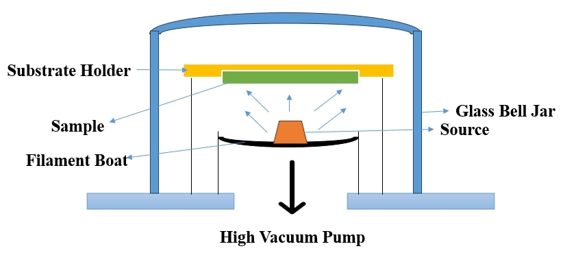
Figure 1. Schematic Diagram of Thermal Evaporation Technique (Re - draw the image[25]).
2.1.1 Working Principle of Thermal Evaporation Technique
The thermal evaporation technique involves the deposition of a thin film on a substrate through the following steps: (1) Material Heating: The target material (e.g., metal) is heated to high temperatures using tungsten wire coils; (2) Vaporization: The high temperature causes the target material to undergo vaporization, turning it into a gaseous state; (3) Vacuum Environment: The process is conducted in a vacuum environment to eliminate interference from air particles and facilitate controlled deposition; (4) Transportation to Substrate: The vaporized material is transported through the vacuum to the substrate where thin film deposition is desired; (5) Condensation: Upon reaching the substrate, the vaporized material condenses on the substrateʼs surface, forming a solid thin film; (6) Solid Film Formation: The condensed material solidifies on the substrate, creating the desired thin film with specific properties[24].
2.2 Sputtering
Sputtering is a versatile physical vapor deposition (PVD) technique used to deposit thin films onto substrates. The fundamental principle of sputtering involves the ejection of atoms from a target material when it is bombarded by energetic ions in a plasma. This process occurs within a vacuum chamber where an inert gas, typically argon, is introduced at low pressure. The ions from the plasma are accelerated towards the target material, causing atoms to be ejected and subsequently deposited onto a substrate, forming a thin film. There are several types of sputtering techniques, including direct current (DC) sputtering, radiofrequency (RF) sputtering, and magnetron sputtering. DC sputtering uses a DC to maintain the plasma and is generally applied to conductive materials. In contrast, RF sputtering utilizes radiofrequency power, making it suitable for non - conductive materials. Magnetron sputtering, which incorporates magnetic fields to confine the plasma near the target, enhances the efficiency of the process, leading to higher deposition rates and improved film quality.
The advantages of sputtering include its versatility in depositing a broad range of materials such as metals, insulators, and semiconductors, as well as its ability to produce uniform coatings over large areas and complex shapes. Sputtering allows precise control over film thickness and composition through the adjustment of process parameters. Recent advancements in sputtering technology have focused on improving target materials and integrating sputtering with other deposition techniques. For instance, Chen and Zhang (2022) provide an overview of the latest developments in sputtering techniques, emphasizing innovations in magnetron sputtering and its applications in various industries[28]. Kumar and Bansal (2023) review the progress in producing high - performance thin films via sputtering, highlighting new materials and process improvements[29]. Additionally, Li and Wang (2023) compare RF and DC sputtering techniques, discussing recent developments and their effects on film quality[30]. Sinha and Singh (2023) explore advancements in magnetron sputtering technology and its diverse applications[31], while Patel and Patel (2023) review recent innovations in sputtering technology, focusing on enhancements in deposition techniques and their impact on thin film coatings[32]. These recent studies underscore the continuous evolution of sputtering technology, reflecting its significant role in the fabrication of thin films for various applications.
Sputtering, a vital PVD process, involves the removal of atoms from a target surface due to high - energy ion bombardment. Unlike evaporation, sputtering does not rely on thermal processes but instead employs ion impact on the target material. Various sputtering processes, such as diode sputtering, reactive sputtering, bias sputtering, magnetron sputtering, and ion - beam sputtering, offer flexibility and performance improvements. Sputtering outperforms evaporation in terms of material choice, substrate adhesion, complex stoichiometries, scalability, and deposition rate[33]. Table 2 summarizes the advantages and disadvantages of the sputtering technology and Figure 2 indicates the Schematic Diagram of sputtering Technique.
Table 2. This Table Provides a Summary of the Advantages and Disadvantages of the Sputtering Technique[30-35]
SL |
Aspect |
Advantages |
Disadvantages |
1 |
Material Choice |
Sputtering outperforms evaporation in terms of material choice, allowing for a broader range of materials to be used in the deposition process. |
Equipment complexity can be high, requiring careful control and monitoring of various parameters. |
2 |
Substrate Adhesion |
Provides excellent substrate adhesion, ensuring that the thin film adheres well to the substrate surface. |
Initial equipment costs can be higher compared to some other deposition techniques. |
3 |
Complex Stoichiometries |
Well - suited for achieving complex stoichiometries in thin films, making it versatile for various applications. |
Sputtering processes may have higher energy consumption, impacting operational costs. |
4 |
Scalability |
Highly scalable, making it suitable for both small - scale and large - scale thin film deposition. |
|
5 |
Deposition Rate |
Generally, offers a higher deposition rate compared to evaporation, allowing for faster production of thin films. |
|
|
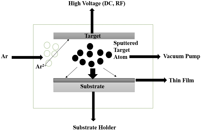
Figure 2. Schematic Diagram of Sputtering Technique (Re - draw the image[35]).
2.2.1 Working Principle of Sputtering
Sputtering is a PVD process that involves the removal of atoms from a target surface due to high - energy ion bombardment. The key steps in sputtering are as follows: (1) Target Material: A target material (e.g., metal) is placed in a vacuum chamber; (2) Ion Bombardment: High - energy ions (usually argon ions) are accelerated towards the target material; (3) Target Atom Ejection: The high - energy ions impact the target surface, causing atoms to be ejected from the target material; (4) Plasma Formation: The ejected atoms form a plasma in the vacuum chamber; (5) Deposition on Substrate: The substrate is placed in close proximity to the target, and the ejected atoms condense on its surface, forming a thin film; (6) Control and Monitoring: The process is carefully controlled, often using techniques like magnetron sputtering or reactive sputtering, and monitored to achieve the desired film characteristics[34].
2.3 CVD
CVD is a widely used technique for depositing thin films and coatings on substrates through chemical reactions involving gaseous precursors. The process involves introducing volatile precursors into a reaction chamber where they undergo chemical reactions to form a solid material that deposits onto a substrate. This technique is highly versatile and can be employed to produce a wide range of materials including metals, semiconductors, and insulators. In a typical CVD process, the substrate is placed in a reaction chamber where it is exposed to gaseous precursors. These precursors react on the substrate surface, often with the aid of heat or plasma, to form a thin film. The deposition parameters such as temperature, pressure, and gas flow rates are carefully controlled to achieve desired film properties such as thickness, uniformity, and composition[36].
Several variations of CVD exist, including Thermal CVD, PECVD, LPCVD, and Metal - Organic CVD (MOCVD). Each variant is suited to different applications based on the material to be deposited and the desired film characteristics. For example, PECVD uses plasma to enhance the chemical reactions, allowing deposition at lower temperatures compared to Thermal CVD, which relies solely on thermal energy[37]. LPCVD operates at lower pressures, which can reduce film stress and improve uniformity over large areas[38]. MOCVD is particularly useful for depositing compound semiconductors and complex materials due to its ability to handle metal - organic precursors[39].
Recent advancements in CVD technology have focused on improving deposition rates, film quality, and scalability. For instance, Zhang et al. (2023) provide a comprehensive review of recent developments in PECVD and its applications in advanced material fabrication[40]. Lee et al. (2022) discuss innovations in LPCVD techniques, highlighting improvements in deposition uniformity and film performance[41]. Additionally, Liu and Xu (2023) explore the latest advancements in MOCVD, including new precursor materials and process optimizations for high - efficiency semiconductor production[42]. These studies underscore the ongoing evolution of CVD technologies and their impact on various fields, from electronics to energy applications. Table 3 summarizes the advantages and disadvantages of the CVD technology and Figure 3 indicates the Schematic Diagram of CVD Technique.
Table 3. Advantages and Disadvantages of CVD Technique[40-46]
SL |
Aspect |
Advantages |
Disadvantages |
1 |
Versatility |
Can be used to deposit films on various materials. |
Some materials may require high temperatures, limiting applicability. |
2 |
Uniform Thin Films |
Provides uniform thin films across the substrate surface. |
The process may have high energy consumption, impacting operational costs. |
3 |
Controlled Deposition |
Allows for control over deposition parameters, influencing film characteristics. |
Best suited for flat substrates, restricting application in three - dimensional structures. |
4 |
Large - Scale Production |
Suitable for large - scale production of thin films. |
|
|
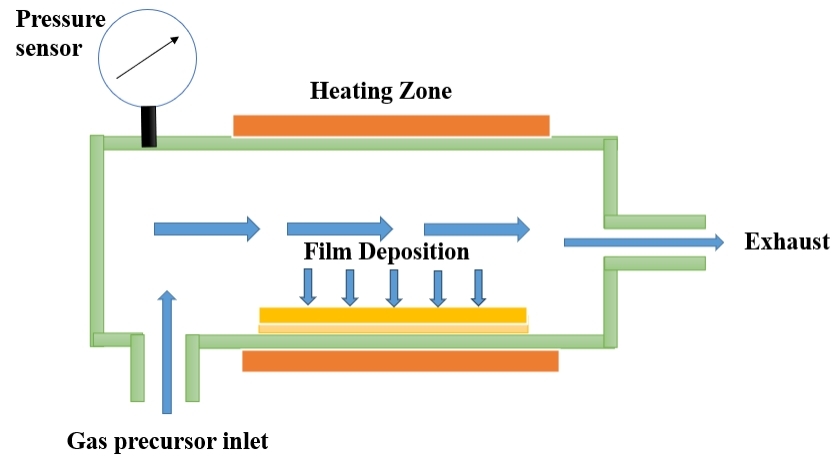
Figure 3. Schematic Diagram of CVD Technique (Re - draw the image[45]).
2.3.1 CVD
CVD is a thin film deposition technique that involves the synthesis of solid materials on a substrate through the chemical reaction of gaseous precursors. The process typically consists of the following key steps[43,44]: (1) Precursor Delivery: Gaseous precursor compounds, containing the elements needed for the desired thin film, are introduced into a reaction chamber; (2) Transport to Substrate: The precursor gases are transported to the substrate where thin film deposition is intended; (3) Activation of Precursors: The precursor molecules are activated, usually by heating or through the use of plasma, to initiate the chemical reactions required for film deposition; (4) Chemical Reactions: The activated precursors undergo chemical reactions on the substrate surface, leading to the formation of solid thin films; (5) Film Growth: As the chemical reactions progress, the thin film grows on the substrate surface, layer by layer; (6) Controlling Parameters: Various parameters, such as temperature, pressure, and precursor flow rates, are carefully controlled to achieve the desired film characteristics; (7) Final Product: Once the deposition process is complete, a solid thin film with specific properties and thickness is formed on the substrate.
2.4 PECVD Technique
PECVD is a widely utilized method for thin - film deposition in fields such as semiconductor fabrication, photovoltaic cells, and optical coatings. PECVD operates at lower temperatures compared to traditional CVD methods by utilizing a plasma to activate chemical reactions. This allows for the deposition of materials on temperature - sensitive substrates while maintaining high film quality.
The PECVD process begins by introducing precursor gases into a vacuum chamber where a plasma is generated using a RF or DC power source. The plasma, consisting of energetic electrons and ions, enables the dissociation of gas molecules into reactive species. These species then interact with the substrate, leading to film formation. The lower operational temperature is a significant advantage of PECVD, as it allows deposition on polymers or other materials that might degrade at high temperatures.
The plasmaʼs role is crucial, as it enhances the chemical reactions that result in the formation of the thin film. The reaction mechanisms in PECVD are governed by surface chemistry, which includes the adsorption, surface diffusion, and reaction of species on the substrate. The plasma’s high - energy environment provides additional energy to the gas molecules, allowing for the dissociation of precursors and facilitating the deposition process at lower temperatures compared to conventional CVD techniques[47].
The deposition rate and film quality in PECVD are influenced by parameters such as gas flow rates, RF power, substrate temperature, and pressure. These parameters must be optimized for specific materials and applications. A notable application of PECVD is in the production of silicon - based thin films, such as hydrogenated amorphous silicon (a - Si), used in solar cells and thin - film transistors[48].
PECVD is also employed for the deposition of dielectric layers, such as silicon dioxide (SiO₂) and silicon nitride (Si₃N₄), which are essential for insulating layers in semiconductor devices. The techniqueʼs versatility extends to the deposition of complex materials, such as doped films or films with gradient compositions, which are useful in various advanced applications, including microelectronics and nanotechnology[49].
2.4.1 Working Principle of PECVD
PECVD technique is a widely used method for depositing thin films, primarily in semiconductor and microelectronics industries, as well as for coating materials with various applications in solar cells, optical coatings, and nanotechnology. The technique operates by enhancing a standard CVD process using plasma, which reduces the necessary deposition temperature[50-55].
(1) Plasma Generation: The PECVD process begins with the generation of a plasma, typically using RF or microwave power, to ionize a gas mixture. This plasma is created by applying an electric field between two electrodes in a vacuum chamber. The gas molecules break into ions, electrons, and radicals, which are highly reactive species that play a key role in the deposition process; (2) Gas Introduction: Reactive gases, such as silane (SiH₄), ammonia (NH₃), methane, or oxygen, are introduced into the deposition chamber. These gases flow continuously into the chamber, where they react with the plasma - generated species; (3) Chemical Reactions: Once the plasma is generated, it activates chemical reactions that lead to the dissociation of precursor gases. The radicals and ions created in the plasma zone react chemically and are transported to the substrate surface. Unlike conventional CVD, PECVD reduces the energy requirements of these reactions, allowing them to occur at much lower temperatures (100-400℃) as opposed to higher temperatures required in standard CVD (~700-1000℃). This makes PECVD ideal for temperature - sensitive substrates like plastics and flexible materials; (4) Thin Film Deposition: The reactive species, once transported to the substrate, adhere to its surface, where they undergo further chemical reactions and condense into a thin film. The film’s properties, such as its thickness, structure, and composition, can be controlled by adjusting process parameters like gas flow rate, pressure, plasma power, and substrate temperature; (5) Applications: PECVD is commonly used for the deposition of Si₃N₄, SiO₂, diamond - like carbon coatings, and other materials for applications in solar cells, LEDs, microelectromechanical systems (MEMS) devices, and protective coatings[52-55].
Table 4 summarizes the advantages and disadvantages of the PECVD technology and Figure 4 indicates the Schematic Diagram of PECVD Technique. Recent research in PECVD has focused on improving film properties such as stress, adhesion, and uniformity, especially for large - scale manufacturing. Advancements in plasma control techniques, such as pulsed PECVD, have led to better control over film composition and microstructure, enabling the development of new materials with tailored properties for specific applications[54].
Table 4. Advantages and Disadvantages of PECVD[52-56]
SL |
Aspect |
Advantages |
Disadvantages |
1 |
Low - Temperature Deposition |
Allows deposition at lower temperatures, making it suitable for heat - sensitive materials. |
Complex equipment setup can be required, leading to higher initial costs. |
2 |
Enhanced Reaction Kinetics |
Plasma activation enhances reaction kinetics, improving film quality. |
Uniformity issues can arise in plasma distribution across the substrate. |
3 |
Versatility in Material Deposition |
Capable of depositing a wide variety of materials, broadening application potential. |
Limited scalability for large - area substrates can be a constraint. |
|
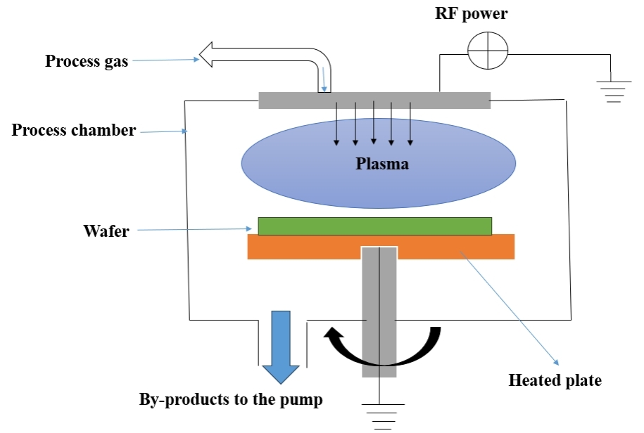
Figure 4. Schematic Diagram of PECVD (Re - draw the image[56]).
2.5 LPCVD
LPCVD is a widely utilized method for thin film deposition in microelectronics and semiconductor manufacturing. This technique operates at lower pressures (typically between 0.1 to 10Torr) compared to conventional CVD processes, which enables better control of film uniformity and reduces the occurrence of defects such as particle formation. LPCVD is particularly favored for its ability to produce high - quality films with excellent step coverage and thickness uniformity, making it ideal for applications such as dielectric, conductor, and semiconductor thin films[57-60].
2.5.1 Working Principle of LPCVD
(1) Gas Introduction: In LPCVD, precursor gases, such as SiH₄, NH₃, or dichlorosilane (SiCl₂H₂), are introduced into a vacuum chamber containing the substrate. The gas flow rate and composition are carefully controlled to ensure optimal conditions for the deposition reaction; (2) Low - Pressure Environment: The vacuum chamber is maintained at a low pressure (below atmospheric pressure), which allows for a reduction in the mean free path of gas molecules. This ensures that the reactive species diffuse slowly towards the substrate, leading to more uniform film deposition across the surface; (3) Thermal Activation: Unlike PECVD, which uses plasma to enhance chemical reactions, LPCVD relies solely on thermal energy. The substrate is heated to a temperature typically in the range of 500-900℃, which provides the necessary energy for the precursor gases to decompose and form a thin film on the substrate; (4) Film Growth: Once the precursor gases reach the substrate surface, they undergo thermal decomposition or chemical reactions to form a solid thin film. For instance, in the deposition of SiO₂, SiH₄ reacts with oxygen at elevated temperatures to produce SiO₂ and hydrogen gas as byproducts. The uniform distribution of the reactive species in the low - pressure environment ensures that the film grows evenly over the entire surface, even in deep trenches or on complex geometries; (5) Applications: LPCVD is commonly used for the deposition of various materials, including polysilicon, silicon dioxide, Si₃N₄, and tungsten. These films are critical in the fabrication of ICs, MEMS, and solar cells. LPCVD’s ability to provide conformal coatings with excellent step coverage makes it ideal for applications where precise film control is required, such as in gate dielectrics, diffusion barriers, and passivation layers[57-62].
Table 5 summarizes the advantages and disadvantages of the LPCVD technology and Figure 5 indicates the Schematic Diagram of LPCVD Technique.
Table 5. Summarizing the Advantages and Disadvantages of LPCVD[62-67]
SL |
Aspect |
Advantages |
Disadvantages |
1 |
Uniformity |
LPCVD provides excellent uniformity and conformity of thin films over large areas and complex surface topographies. |
LPCVD typically requires high temperatures (500-900℃), which may limit its use on temperature - sensitive substrates. |
2 |
High - Quality Films |
Produces high - purity, dense, and high - quality films due to the controlled reaction environment and reduced contamination risk in a low - pressure system. |
The deposition rate is generally slower compared to other CVD methods, which may affect throughput. |
3 |
Low Defect Density |
Films grown using LPCVD exhibit low defect density, which is beneficial for semiconductor devices and MEMS applications. |
The equipment required for LPCVD is more expensive and complex compared to simpler techniques like thermal evaporation. |
4 |
Scalability |
The process is highly scalable, making it suitable for batch processing, which is efficient and cost - effective for industrial applications. |
Films deposited at high temperatures can sometimes exhibit internal stresses, which may impact mechanical properties. |
5 |
Versatility |
LPCVD can be used to deposit a wide range of materials, including oxides, nitrides, polysilicon, and others. |
The use of hazardous or toxic precursor gases (e.g., silane, phosphine) can require stringent safety measures and proper waste management. |
|
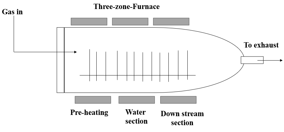
Figure 5. Schematic Diagram of LPCVD (Re - draw the image[62]).
2.6 MBE
MBE is a highly controlled, ultra - high vacuum (UHV) deposition technique widely used for the growth of high - purity crystalline thin films, particularly for semiconductor materials. The fundamental principle of MBE involves the slow and precise deposition of atoms or molecules onto a heated substrate, where they form a crystalline structure layer by layer. Unlike other deposition methods, MBE operates at extremely low deposition rates, which allows for unparalleled control over the thickness, composition, and crystal quality of the films.
In MBE, the material sources, typically in the form of high - purity elemental compounds, are heated in effusion cells, creating beams of atoms or molecules that travel through the UHV environment and impinge on the substrate surface. The slow deposition rates (on the order of one monolayer per second) enable atomic - level control over the growth process, making MBE ideal for fabricating complex heterostructures, quantum wells, superlattices, and other advanced nanostructures. The use of UHV conditions minimizes contamination, allowing for the growth of extremely pure films.
A key advantage of MBE is its ability to grow films with atomically sharp interfaces and precise doping profiles, which are essential in electronic and optoelectronic devices. The technique is particularly suited for materials like III-V semiconductors (e.g., gallium arsenide, InP), where precise control over layer composition is crucial for device performance. Real - time monitoring of the growth process can be achieved using reflection high - energy electron diffraction (RHEED), providing insight into the surface structure and growth dynamics during deposition.
Recent advancements in MBE focus on expanding its applications beyond traditional semiconductors, including the growth of complex oxides, two - dimensional materials, and topological insulators. These new materials offer potential applications in next - generation electronics, spintronics, and quantum computing. For example, Chen et al. (2022) explore the use of MBE for the growth of two - dimensional transition metal dichalcogenides and their applications in nanoelectronics and optoelectronics[68]. Additionally, Wang et al. (2023) review the application of MBE in fabricating complex oxide heterostructures for emerging electronic devices[69]. MBE remains a cutting - edge technique in thin film growth, offering unmatched precision and flexibility in material deposition for advanced applications[70].
MBE is a precise deposition technique that involves evaporating individual atoms or molecules from a solid source to form a crystalline film layer on a substrate. This method provides exceptional control over film thickness and composition, making it particularly suitable for semiconductor device fabrication[71]. Table 6 summarizes the advantages and disadvantages of the MBE technology and Figure 6 indicates the Schematic Diagram of MBE Technique.
Table 6. Advantages and Disadvantages of Molecular Beam Epitaxy Technique[69-75]
SL |
Aspect |
Advantages |
Disadvantages |
1 |
Precision |
Offers precise control over film thickness and composition at the atomic level. |
MBE systems are complex and require advanced technical expertise. |
2 |
Crystalline Film Formation |
Produces crystalline films with high structural quality. |
Typically has lower deposition rates compared to some other techniques. |
3 |
Semiconductor Fabrication |
Particularly suitable for semiconductor device fabrication due to its precision. |
The initial setup costs can be relatively high. |
4 |
Low Contamination |
Low contamination risk due to the ultra - high vacuum environment. |
May be less scalable for large - area deposition compared to other methods. |
|
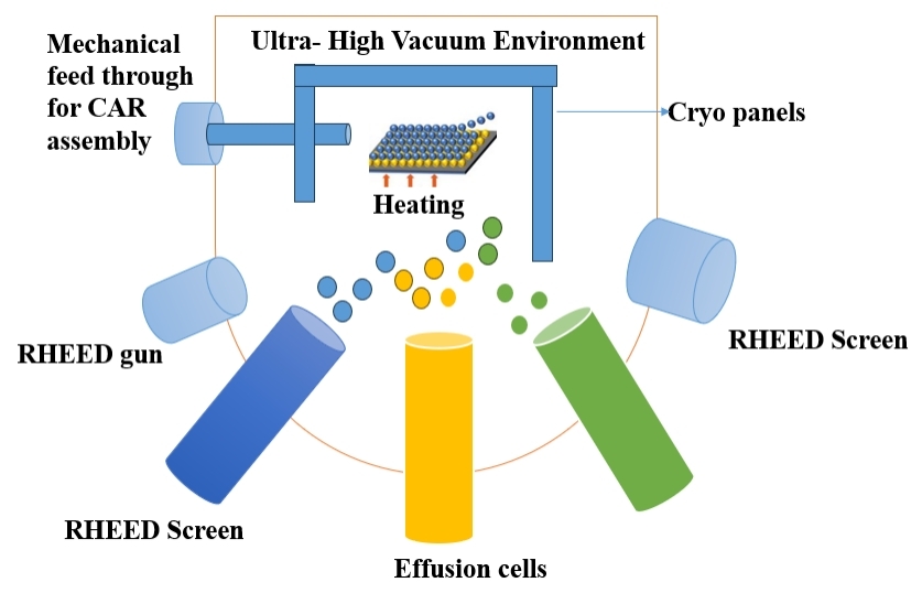
Figure 6. Schematic Diagram of Molecular Beam Epitaxy Technique (Re - draw the image[74]).
2.6.1 MBE
MBE is a highly precise thin film deposition technique used for the growth of crystalline films with atomic - level accuracy. The process involves the deposition of individual atoms or molecules from a solid source onto a substrate. The working principle of MBE can be outlined in the following steps: (1) UHV Environment: MBE takes place in an UHV environment to minimize any interference from background gases and to ensure a clean substrate surface; (2) Effusion Cells: Sources of the desired material, typically in the form of effusion cells, are heated to high temperatures. These cells contain the solid material (typically a metal) that will be evaporated for deposition; (3) Thermal Evaporation: The high temperatures cause the solid material in the effusion cells to evaporate, forming a molecular or atomic beam; (4) Collimation and Directional Beam: The evaporated material forms a collimated beam, ensuring that the atoms or molecules move in a specific, well - defined direction toward the substrate; (5) Substrate Interaction: The substrate is positioned in the path of the molecular or atomic beam. As the evaporated material reaches the substrate, it forms a monolayer on the surface; (6) Layer - by - Layer Growth: MBE operates in a layer - by - layer fashion, allowing precise control over the thickness and composition of the deposited film. This is achieved by alternating the deposition of different materials in a controlled sequence; (7) Real - Time Monitoring: The growth process is often monitored in real - time using various techniques, such as RHEED, to assess the crystal quality and adjust growth conditions accordingly; (8) Controlled Stoichiometry: MBE enables the deposition of films with controlled stoichiometry, ensuring that the desired chemical composition is achieved; (9) Substrate Rotation and Manipulation: Substrate rotation and manipulation systems allow for uniform film growth and the creation of complex structures.
MBE is especially valued in the fabrication of semiconductor devices and heterostructures due to its ability to precisely control film thickness, composition, and crystalline structure at the atomic level. The UHV environment and careful control of deposition conditions contribute to the high purity and quality of the resulting thin films[70-75].
2.7 ALD
ALD is a vapor - phase thin film deposition technique that allows for the precise, layer - by - layer construction of materials with atomic - level control. ALD operates on the principle of sequential, self - limiting chemical reactions between gaseous precursors and a substrate surface. This unique mechanism distinguishes ALD from other deposition techniques by enabling unparalleled uniformity and thickness control, even on complex geometries and high aspect ratio structures.
In a typical ALD process, the deposition cycle consists of two half - reactions. In each half - reaction, one of the precursor gases is introduced to the substrate, where it reacts with the surface to form a monolayer of material. This is followed by purging the chamber to remove any unreacted precursor and by - products. Then, a second precursor is introduced, reacting with the previously adsorbed monolayer, forming a thin film. The cycle is repeated multiple times to achieve the desired thickness, with each cycle depositing a controlled amount of material, usually on the order of one atomic layer per cycle.
The self - limiting nature of ALD makes it particularly well - suited for applications where conformality and precise thickness control are critical. ALD is widely used in the semiconductor industry for the deposition of thin dielectric layers, such as high - k oxides (e.g., Al₂O₃, HfO₂), which are essential for modern transistors and capacitors. Additionally, ALD has been employed in energy storage devices, protective coatings, and biomedical applications. The high - quality films produced by ALD exhibit excellent step coverage and uniformity, even on substrates with intricate topographies.
Recent advancements in ALD include the development of plasma - enhanced ALD (PEALD), which enables deposition at lower temperatures, expanding the range of substrate materials that can be used. Moreover, spatial ALD has gained attention for its higher throughput capabilities, making it more suitable for industrial - scale applications. According to Kunene et al. (2022), ALD is now being integrated into the fabrication processes of next - generation nanoelectronics, particularly in the deposition of 2D materials and nanostructures for high - performance transistors[76]. Similarly, Yang et al. (2023) emphasizes the role of ALD in improving the energy storage capacity of lithium - ion batteries by coating electrode materials with ultra - thin, conformal layers to enhance stability and performance[77,78].
Overall, ALD remains a critical tool for applications that require thin, highly conformal films with precise thickness control and is expected to play a growing role in the development of future technologies, particularly in the fields of electronics, energy storage, and nanotechnology.
ALD is a technique that allows for the controlled deposition of thin films with atomic - scale precision. It involves the sequential exposure of a substrate to precursor gases, resulting in self - limiting surface reactions that lead to the formation of thin films. ALD is widely used in applications requiring precise thickness control, such as microelectronics and nanotechnology[79]. Table 7 summarizes the advantages and disadvantages of the ALD technology and Figure 7 indicates the Schematic Diagram of ALD Technique.
Table 7. Advantages and Disadvantages Atomic Layer Deposition Technique[80-83]
SL |
Aspect |
Advantages |
Disadvantages |
1 |
Atomic - Scale Precision |
Provides precise control over film thickness at the atomic level. |
Generally, has a slower deposition rate compared to some other techniques. |
2 |
Conformal Coating |
Achieves conformal coating on complex geometries and high - aspect - ratio structures. |
Involves a complex sequential process, which can increase processing time. |
3 |
High Uniformity |
Offers high uniformity in film thickness across the substrate. |
The initial setup costs can be relatively high. |
4 |
Wide Material Compatibility |
Compatible with a variety of materials. |
Not suitable for all materials, and precursor availability can be a limiting factor. |
|
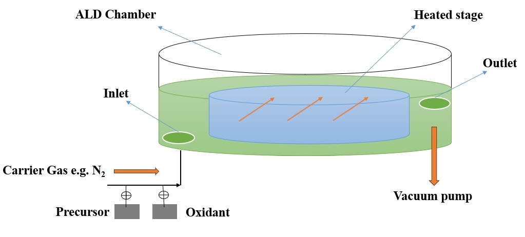
Figure 7. Schematic Diagram of ALD (Re - draw the image[81]).
2.7.1 Working Principle of ALD
ALD is a thin film deposition technique that enables the controlled and precise growth of thin films with atomic - scale precision. The working principle of ALD involves a sequential, self - limiting surface reaction process, and it typically follows these key steps: (1)Substrate Preparation: The substrate, on which the thin film will be deposited, is thoroughly cleaned to ensure a clean and reactive surface; (2) Sequential Exposure to Precursors: The substrate is exposed sequentially to gaseous precursor compounds in a cyclic manner. Each precursor is introduced one at a time, and the exposure is carefully controlled; (3) Adsorption of Precursors: The first precursor is introduced, forming a monolayer of adsorbed molecules on the substrate surface. The adsorption occurs due to chemical reactions with the surface functional groups; (4) Self - Limiting Reaction: The chemical reaction is self - limiting, meaning that it saturates the surface and forms a complete monolayer. This ensures precise control over film thickness; (5) Purge Step: Excess precursor and reaction by - products are removed from the reaction chamber through a purge step, often involving inert gas flow. This step is crucial to prevent unwanted reactions in the subsequent cycle; (6) Sequential Introduction of Second Precursor: The process is repeated with a second precursor, which reacts with the adsorbed molecules on the substrate surface, forming another self - limiting monolayer; (7) Cycle Repetition: The sequential exposure and purge steps are repeated for each precursor in a cycle until the desired film thickness is achieved. The number of cycles determines the thickness with atomic precision; (8) Film Growth and Composition Control: The repeated cycles result in the controlled growth of the thin film. By choosing different precursor combinations and cycle parameters, the composition of the film can be precisely controlled; (9) Uniformity and Conformality: ALD is known for providing excellent uniformity and conformality, ensuring that the thin film conforms to complex substrate geometries and structures.
ALD is widely used in various applications, particularly in microelectronics and nanotechnology, where precise control over film thickness and composition is critical. The self - limiting nature of the process and the ability to achieve atomic - scale precision make ALD a powerful technique for advanced material fabrication[80].
2.8 CBD Technique
CBD is a simple, cost - effective method used to deposit thin films from an aqueous solution. In this technique, a substrate is immersed in a solution containing the precursor ions, and a thin film is gradually deposited onto the substrate through a series of chemical reactions that occur in the solution. CBD is primarily used for the deposition of metal chalcogenides and oxides, such as ZnO, CdS, and PbS, which are extensively studied for their applications in solar cells, sensors, and optoelectronic devices. The process relies on the controlled precipitation of the target material on the substrate surface from a solution under carefully regulated conditions. The deposition is initiated by supersaturation of the solution, which can be controlled by adjusting parameters such as temperature, pH, and the concentration of the precursors. In many cases, complexing agents like ammonia are added to the solution to control the release rate of metal ions, allowing for a more uniform film growth. For example, in the deposition of ZnO, zinc ions are slowly released and react with hydroxide ions to form a ZnO layer on the substrate. CBD offers several advantages, such as low - cost equipment, simplicity, and the ability to coat large areas and complex shapes. It is particularly attractive for large - scale production of thin films on various substrates, including glass, polymers, and metals. However, the techniqueʼs limitations include relatively slow deposition rates, poor film adhesion in some cases, and challenges in controlling the filmʼs stoichiometry and uniformity.
Recent advancements in CBD have focused on improving film quality and expanding its applicability. Studies have demonstrated the deposition of high - quality films with enhanced optical and electrical properties by optimizing the deposition parameters. Moreover, nanostructured films, such as nanorods and nanoparticles, have been successfully fabricated using CBD for use in next - generation photovoltaic devices and nanotechnology applications. According to Ali et al. (2022), CBD has been widely employed in the fabrication of buffer layers for thin - film solar cells, such as CdS layers for Cu(In,Ga)Se₂ (Copper Indium Gallium Selenide) and CdTe solar cells, enhancing their efficiency and stability[84]. Additionally, research by Singh et al. (2023) highlights the use of CBD in producing ZnO - based nanostructures with enhanced gas - sensing properties, demonstrating the techniqueʼs versatility in developing functional materials[2].
In conclusion, CBD remains a vital technique for the deposition of thin films, particularly in the context of large - area applications and the synthesis of nanostructured materials. Its simplicity, low cost, and versatility make it a valuable tool in various fields, from photovoltaics to sensor technology Chemical bath deposition, also known as the solution growth technique, is an established method for depositing films on substrates. This technique is commonly used for chalcogenide and metal oxide films at lower temperatures. Precursor solutions complexed by ligands, such as ammonia, triethanolamine, or ethylene - diamine - tetra acetic acid, facilitate the deposition process. The chemical bath deposition method provides versatility for vertical, horizontal, or specific substrate positions, allowing the achievement of desired film thicknesses[85]. Table 8 summarizes the advantages and disadvantages of the CBD technology and Figure 8 indicates the Schematic Diagram of CBD Technique.
Table 8. Advantages and Disadvantages Chemical Bath Deposition Technique[85-93]
SL |
Aspect |
Advantages |
Disadvantages |
1 |
Low - Temperature Process |
Suitable for depositing films at lower temperatures, reducing thermal stress on substrates. |
May not achieve the same level of control over film properties as some other techniques. |
2 |
Versatility |
Allows for deposition on vertical, horizontal, or specific substrate positions. |
Suited for specific materials, limiting its range of applications. |
3 |
Cost - Effective |
Generally, has lower initial equipment costs compared to some other techniques. |
May have challenges achieving uniform coating on complex surfaces. |
4 |
Ease of Operation |
Generally considered simpler and more straightforward to operate. |
Typically has slower deposition rates compared to some high - temperature techniques. |
|
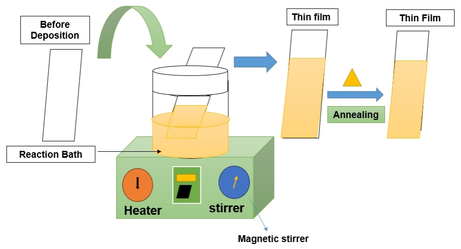
Figure 8. Schematic Diagram of CBD (Re - draw the image[90]).
2.8.1 Working Principle of CBD
CBD, also referred to as the solution growth technique, is employed for depositing thin films on substrates, particularly for chalcogenides and metal oxides, at lower temperatures. The operational steps include: Preparation of Precursor Solutions: Precursor solutions are formulated by dissolving chemical compounds in a solvent, often complexed with ligands like ammonia or triethanolamine; (2) Substrate Immersion: The substrate, intended for thin film deposition, is immersed in the prepared precursor solution; (3) Chemical Reaction and Film Formation: Chemical reactions in the solution lead to the formation of solid particles or material complexes, adhering to the substrate surface and initiating thin film growth; (4) Substrate Positioning: The substrate can be oriented vertically, horizontally, or in a specific manner to control film thickness and coverage; (5) Bath Composition Control: Parameters such as bath composition, temperature, and immersion time are meticulously regulated to manage the deposition process; (6) Rinsing and Drying: After the deposition period, the substrate is removed, rinsed to eliminate excess reactants, and then dried; (7) Versatility and Film Properties: CBD provides versatility in substrate positioning and is applicable to various film compositions. However, achieving precise control over film properties may be challenging compared to alternative deposition techniques.
Chemical Bath Deposition is acknowledged for its cost - effectiveness, simplicity, and lower equipment costs. It is chosen for applications prioritizing low - temperature processing and operational ease over highly precise film characteristics. While it may not offer the same level of control as some techniques, CBD is valuable for specific materials and applications[86-90].
3 CONCLUSION
In this review, the various thin - film deposition techniques, including thermal evaporation, sputtering, CVD, MBE, ALD, CBD, LPCVD, and PECVD, have been discussed in detail. Each of these techniques offers distinct advantages and disadvantages, making them suitable for different applications in industries such as semiconductors, photovoltaics, optoelectronics, and sensors. Thermal evaporation remains a widely used method for large - scale production of semiconductors due to its simplicity and ability to deposit thin films with minimal interference. However, its limitations include uniformity challenges and high energy consumption, which may restrict its use for more complex or three - dimensional substrates. Sputtering techniques, on the other hand, offer improved control over film uniformity and are capable of handling a wider range of materials, but require more sophisticated equipment and higher operational costs. CVD techniques, including LPCVD and PECVD, continue to be pivotal in industries requiring high - quality films with precise control over thickness and composition. LPCVD is commonly used for microelectronics and MEMS fabrication, whereas PECVD is known for producing thin films at lower temperatures, making it ideal for temperature - sensitive substrates. MBE and ALD, though more complex and costly, provide atomic - level precision in deposition, which is essential for advanced nanotechnology and semiconductor applications. CBD offers a cost - effective and straightforward method for depositing films from solution, particularly for large - area applications. However, its relatively slow deposition rate and challenges with film uniformity can limit its effectiveness in certain high - performance applications.
Recent advancements in these deposition techniques have focused on improving the quality and performance of thin films, while also addressing the limitations associated with each method. The development of hybrid and advanced deposition techniques, such as combining CVD with other methods, is an exciting area of research that aims to enhance the capabilities of thin - film fabrication. In conclusion, the selection of a deposition technique is highly dependent on the specific application and material requirements. Future research is expected to focus on optimizing these techniques for better material properties, scalability, and cost - effectiveness. As industries continue to demand higher performance materials with precise control over properties, thin - film deposition technologies will remain at the forefront of scientific and industrial innovation.
Acknowledgements
Authors would like to thank to Bangladesh Atomic Energy Commission, and Technical Teachers’ Training College, Ministry of Education, People’s Republic of Bangladesh for their inspiration to complete this work.
Conflicts of Interest
The authors declared no conflict of interest.
Author Contribution
Toma FTZ and Rahman MS prepared the original draft and wrote reviewed the manuscript. Ahmed S edited the manuscript and Hussain KMA supervised to complete the manuscript. All authors read and approved the manuscript for submission.
Abbreviation List
ALD, Atomic layer deposition
CBD, Chemical bath deposition
CVD, Chemical vapor deposition
DC, Direct current
ICs, Integrated circuits
LPCVD, Low-pressure chemical vapor deposition
MBE, Molecular beam epitaxy
MEMS, Microelectromechanical systems
MOCVD, Metal-organic chemical vapor deposition
NH₃, Ammonia
PECVD, Plasma-enhanced chemical vapor deposition
PVD, Physical vapor deposition
RF, Radio frequency
RHEED, Reflection high-energy electron diffraction
Si₃N₄, Silicon nitride
SiH₄, Silane
SiO₂, Silicon dioxide
UHV, Ultra-high vacuum
References
[2] Benson K, Thompson R. Sputtering techniques for thin film deposition: A review. Surf Coat Tech, 2023; 459: 128500.
[3] Kumar A, Kaur K. Low-pressure chemical vapor deposition for advanced materials: Principles and applications. J Mater Res, 2022; 37: 1235-1245.
[4] Zhang X. Plasma-enhanced chemical vapor deposition for semiconductor thin films: Recent advancements and future directions. J Vac Sci Technol, 2023; 41: 031204.
[5] Voss J, Leister H. Molecular beam epitaxy: Principles, applications, and future prospects. J Cryst Growth, 2023; 586: 126679.
[6] Kang H. Atomic layer deposition of high-k dielectrics: Fundamentals and applications. J Mater Res, 2021; 36: 2119-2141.
[7] Ali H. Advances in chemical bath deposition for metal chalcogenide thin films: A review. Sol Energ Mat Sol C, 2022; 246: 111904.
[8] Smith J. Sustainable practices in thin film deposition: A review. Environ Sci Technol, 2023; 57: 1301-1320.
[9] Choi J. A review on the application of MBE in advanced semiconductor fabrication. J Appl Phys, 2023; 133: 081101.
[10] Chen T. Review of recent advancements in CVD techniques for functional materials. Mater Today, 2022; 51: 120-139.
[11] Li Y. Progress in ALD techniques for energy applications. Energ Environ Sci, 2022; 15: 1853-1874.
[12] Park J. The role of thin film technologies in modern solar cell fabrication. Renew Sust Energ Rev, 2022; 146: 111111.
[13] Zhao M. Advances in flexible thin film deposition technologies. Mater Today P, 2023; 57: 402-407.
[14] Yang H. Recent developments in the synthesis of nanostructured materials via CBD. Nanoscale Adv, 2022; 4: 3491-3505.
[15] Kim S. Thin film deposition methods: An overview of their principles and applications. Prog Mater Sci, 2023; 132: 100988.
[16] Khan Y, Akhtar S, Bafakeeh OT. Recent Advances in Thermal Evaporation Techniques for Thin Film Deposition: A Review. J Mater Sci Technol, 2023; 102: 11-26.
[17] Ali S, Zhang Y. Thermal Evaporation and Its Applications in Thin Film Technology: A Comprehensive Review. Mater Today P, 2023; 54: 190-204.
[18] Nguyen T, Lee JH. Enhancing Thin Film Properties through Advanced Thermal Evaporation Techniques. J Vac Sci Technol A, 2023; 41: 031203.
[19] Lee HS, Yang SH. Optimization of Thermal Evaporation Processes for High-Performance Thin Films. Thin Solid Films, 2023; 738: 139174.
[20] Kumar R, Sharma A. Recent Trends in Thermal Evaporation for Thin Film Deposition: Advances and Challenges. Mat Sci Eng R, 2023; 146: 100639.
[21] Reddy MA, Kumar PS. Thermal Evaporation Technique: Recent Advances and Applications in Electronics and Photonics. Prog Mater Sci, 2023; 119: 100774.
[22] Messier. Thin Film Deposition Processes. MRS Bull, 1988; 13: 18-21.[DOI]
[23] Soonmin H. Thermal Evaporation of Thin Films: Review. Middle-East J Sci Res, 2015; 23: 2695-2699.
[24] Mattox D. The Foundations of Vacuum Coating Technology. Springer Publishing: Berlin, Germany, 2004.
[25] Tyagi P, Johan MR, Bin Johan MR. Titanium dioxide / graphene composites for dye-sensitized solar cell applications. Green Sust Proc Chem Environ Eng Sci, 2022; 2022: 313-339.[DOI]
[26] Trontl V, Pletikosić I, Milun M et al. Experimental and ab initio study of the structural and electronic properties of subnanometer thick Ag films on Pd(111). Phys Rev B, 2005; 72: 235418.[DOI]
[27] Neilsen W. World Catalog of the Beach-Fly Family Canacidae (Diptera). Mathis, 1992; 12: 1-7.[DOI]
[28] Chen X, Zhang H. Advances in Sputtering Deposition Techniques for Thin Film Fabrication. J Vac Sci Technol A, 2022; 40: 051203.
[29] Kumar P, Bansal V. High-Performance Thin Films via Sputtering: Recent Progress and Challenges. Thin Solid Films, 2023; 751: 139204.
[30] Li Z, Wang Y. Radio Frequency and Direct Current Sputtering Techniques: A Comparative Study and Recent Developments. Surf Coat Tech, 2023; 423: 127323.
[31] Sinha S, Singh A. Magnetron Sputtering for Thin Film Deposition: Advances and Applications. Prog Vacuum Sci Techno, 2023; 7: 015001.
[32] Patel R, Patel N. Recent Innovations in Sputtering Technology for Thin Film Coatings. Mater Today, 2023; 65: 27-34.
[33] Westwood WD. Sputter Deposition. American Vacuum Society Education Committee Press: New York, USA, 2003.
[34] Berg S, Nyberg T. Fundamental understanding and modeling of reactive sputtering processes. Thin Solid Films, 2005; 476: 215-230.[DOI]
[35] Yoon Y, Jung J. Characterization of the Vanadium Alloy Thin Films Coated by Sputtering. Korean Chem Eng Res, 2016; 54: 598-605.[DOI]
[36] Ishii K. High-rate low kinetic energy gas-flow-sputtering system. J Vac Sci Technol A, 1989; 7: 256-258.[DOI]
[37] Zhang Y. Recent Advances in Plasma-Enhanced Chemical Vapor Deposition for Advanced Materials. J Vac Sci Technol A, 2023; 41: 031202.
[38] Lee J. Low-Pressure Chemical Vapor Deposition: Recent Developments and Applications. Thin Solid Films, 2022; 755: 139108.
[39] Liu J, Xu L. Metal-Organic Chemical Vapor Deposition: Innovations and Applications. Surf Coat Tech, 2023; 428: 127609.
[40] Zhang H. Review of Plasma-Enhanced Chemical Vapor Deposition Process, Application, and Challenges. Mater Today, 2023; 65: 243-252.
[41] Lee S. Advancements in Low-Pressure Chemical Vapor Deposition Techniques for Uniform Thin Film Growth. J Mater Sci, 2022; 58: 5412-5423.
[42] Liu Y, Xu W. Recent Trends in Metal-Organic Chemical Vapor Deposition for Semiconductor Devices. J Cryst Growth, 2023; 597: 125870.
[43] Shareef IA, Rubloff GW, Anderle M et al. Sub atmospheric chemical vapor deposition ozone/TEOS process for SiO2 trench filling. J Vac Sci Technol B, 1995; 13: 1888-1892.[DOI]
[44] Murakami K, Tanaka S, Hirukawa A et al. Direct synthesis of large area graphene on insulating substrate by gallium vapor-assisted chemical vapor deposition. Appl Phys Lett, 2015; 106: 093112.[DOI]
[45] Zhang Q, Sando D, Nagarajan V. Chemical route derived bismuth ferrite thin films and nanomaterials. J Mater Chem C, 2016; 4: 4092-4124.[DOI]
[46] Zhang C, Lin W, Zhao Z et al. CVD synthesis of nitrogen-doped graphene using urea. Sci China Phys Mech, 2015; 58: 107801.[DOI]
[47] Sharma V. Plasma-enhanced chemical vapor deposition: Process and applications. J Appl Phys, 2021; 125: 050902.
[48] Kuech TF. Low-temperature PECVD for thin-film silicon applications. Mat Sci Semicon Proc, 2022; 103: 106-111.
[49] Radamson HB. Recent developments in PECVD technologies for dielectric film deposition. Microelectron J, 2023; 89: 56-65.
[50] Vargas-Bernal JR. Pulsed PECVD and its application in advanced material deposition. Vacuum, 2023; 209: 110-118.
[51] Hari SD. Recent Advances in Plasma-Enhanced Chemical Vapor Deposition for Thin-Film Solar Cells. Sol Energ Mat Sol C, 2024; 246: 111898.
[52] Michon A. Plasma Enhanced Chemical Vapor Deposition for the Synthesis of Advanced Materials: Recent Developments and Applications. Mater Today, 2023; 66: 15-30.
[53] Roy B. Low-Temperature PECVD Process for Flexible Electronics Applications: An Overview. Appl Surf Sci, 2023; 628: 157517.
[54] Li X. Advances in PECVD Techniques for the Deposition of Thin Films in Microelectronics. J Vac Sci Technol B, 2023; 41: 010801.
[55] Singh RK. The Role of PECVD in Advanced Semiconductor Manufacturing. Ieee T Semiconduct M, 2023; 36: 309-318.
[56] Chena B, Tay FE, Iliescu C. Development of thick film PECVD Amorphous silicon with low stress for MEMS applications. Proc of SPIE, 2008; 7269: 1-11.[DOI]
[57] Lee SY. Recent Advances in LPCVD Processes for Thin Film Deposition in Semiconductor Manufacturing. J Vac Sci Technol A, 2023; 41: 031101.
[58] Singh R. Low-Pressure Chemical Vapor Deposition of Silicon Nitride Films for Advanced Microelectronic Applications. Appl Surf Sci, 2023; 639: 158279.
[59] Park M. Enhancing Conformal Coating Performance in LPCVD: New Insights and Techniques. Mat Sci Semicon Proc, 2024; 157: 106799.
[60] Gupta AK. LPCVD in Nanotechnology: Deposition of Metal Oxides for High-Performance Devices. Mater Today, 2024; 68: 220-228.
[61] Kedzierski FJ. LPCVD Processes for Next-Generation MEMS Devices: A Review. J Microelectromech S, 2023; 32: 765-772.
[62] Chawla N, Nagarajan R, Bhattacharya E. Experimental and Theoretical Investigation of Thermodynamic and Transport Phenomena in Polysilicon and Silicon Nitride CVD. Ecs T, 2009; 19: 19-23.[DOI]
[63] Ramanathan S. Introduction: Thin Film Deposition Processes and Technologies: Chemical Vapor Deposition (CVD). In: Encyclopedia of Materials: Science and Technology. Elsevier Publishing: Netherlands, 2009; 4-110.
[64] Kern W, Puotinen D. Cleaning Solutions Based on Hydrogen Peroxide for Use in Silicon Semiconductor Technology. Rca Rev, 1970; 31: 187-206.
[65] Seshan K. Handbook of Thin Film Deposition Techniques Principles, Methods, Equipment, and Applications. Elsevier Publishing: Amsterdam, Netherlands, 2012.
[66] Pai MR, Manivannan A. Low-Pressure Chemical Vapor Deposition (LPCVD) of Thin Films. J Electrochem Soc, 2009; 156: 32-45.
[67] Park HJ. Low Pressure Chemical Vapor Deposition of Silicon Nitride and Polysilicon Films for Advanced MEMS Applications. Microelectron J, 2017; 63: 34-42.
[68] Chen S. Molecular Beam Epitaxy of 2D Transition Metal Dichalcogenides for Nanoelectronics and Optoelectronics. J Appl Phys, 2022; 132: 231501.
[69] Wang Z. MBE-Grown Complex Oxide Heterostructures: Applications and Challenges in Emerging Electronics. Adv Mater, 2023; 35: 2301043.
[70] Jones R, Smith T. Advances in Molecular Beam Epitaxy for Semiconductor Device Fabrication. Semicond Sci Tech, 2023; 38: 085006.
[71] Aeger RC. Introduction to Microelectronic Fabrication, 2nd ed. Prentice Hall Publishing: Upper Saddle River, USA, 2002.
[72] McCray WP. MBE Deserves a Place in the History Books. Nat Nanotechnol, 2007; 2: 259-261.[DOI]
[73] Shchukin VA, Bimberg D. Spontaneous ordering of nanostructures on crystal surfaces. Rev Mod Phys, 1999; 71: 1125-1171.[DOI]
[74] Wu G, Wang Y, Gong Q et al. An intelligent temperature control algorithm of Molecular Beam Epitaxy system based on the Back-Propagation neural network. Ieee Access, 2016; 4: 1-8.[DOI]
[75] Stangl J, Holý V, Bauer G. Structural properties of self-organized semiconductor nanostructures. Rev Mod Phys, 2004; 76: 725-783.[DOI]
[76] Kunene TJ, Tartibu LK, Ukoba K et al. Review of Atomic Layer Deposition Process, Application, and Modeling Tools. Mater Today Proc, 2022; 62: S95-S100.[DOI]
[77] Yang X. Advances in Atomic Layer Deposition for Energy Storage: Conformal Coatings and Interface Engineering. Nano Energy, 2023; 105: 108304.
[78] Lee H. Atomic Layer Deposition for High-Performance 2D Materials and Heterostructures. J Mater Sci, 2023; 58: 4573-4584.
[79] Oviroh PO, Akbarzadeh R, Pan D et al. New Development of Atomic Layer Deposition: Processes, Methods, and Applications. Sci Technol Adv Mat, 2019; 20: 465-496.[DOI]
[80] Puurunen RL. Surface chemistry of atomic layer deposition: A case study for the trimethylaluminum/water process. J Appl Phys, 2005; 97: 121301.[DOI]
[81] TziaMingOnn R, Küngas R, Fornasiero P et al. Atomic Layer Deposition on Porous Materials: Problems with Conventional Approaches to Catalyst and Fuel Cell Electrode Preparation. Inorganics, 2018; 6: 34.[DOI]
[82] Miikkulainen V, Leskelä M, Ritala M et al. Crystallinity of inorganic films grown by atomic layer deposition: Overview and general trends. J Appl Phys, 2013; 113: 021301.[DOI]
[83] Potts SE, Kessels WM. Energy-enhanced atomic layer deposition for more process and precursor versatility. Coordin Chem Rev, 2013; 257: 3254-3270.[DOI]
[84] Ali MS. Chemical Bath Deposition of Buffer Layers for High-Efficiency Thin-Film Solar Cells. Sol Energ Mat Sol C, 2022; 239: 111691.
[85] Singh R. Nanostructured ZnO Films Deposited by Chemical Bath Deposition for Gas-Sensing Applications. J Alloy Compd, 2023; 947: 169562.
[86] Patil A. Recent Advances in Chemical Bath Deposition for Thin Film Solar Cells. Mater Today Proc, 2023; 72: 2543-2547.
[87] Zia R, Riaz M, Anjum S. Study the effect of thiourea concentration on optical and structural properties of CdS-nanocrystalline thin films prepared by CBD technique. Optik, 2016; 127: 5407-5412.[DOI]
[88] Kwon J, Ahn J, Yang H. Chemical bath deposition of CdS channel layer for fabrication of low temperature-processed thin-film-transistors. Curr Appl Phys, 2013; 13: 84-89.[DOI]
[89] Toma F, Hussain K, Rahman M et al. Preparation and characterization of CdS thin film using chemical bath deposition (CBD) technique for solar cell application. World J Adv Res Rev, 2021; 12: 629-633.[DOI]
[90] Shaikh S, Inamdar S, Ganbavle V et al. Chemical bath deposited ZnO thin film-based UV photoconductive detector. J Alloy Compd, 2016; 664: 242-249.[DOI]
[91] Toma F, Rahman M, Hussain K et al. Effect of the Annealing Temperature on CdS Nanoparticles Synthesized by Chemical Precipitation Technique and also Characterized for its Potential Technological Applications. Nano Trends, 2021; 23: 20-28.
[92] Ahmed Z, Rahman MT, Hussain K et al. Characterization and Optimization of ZnS Thin Film Properties Synthesis via Chemical Bath Deposition Method for Solar Cell Buffer Layer. J Main Group Chem, 2023; 22: 79-91.[DOI]
[93] Sumaya MU, Maria KH, Toma F et al. Effect of stabilizer content in different solvents on the synthesis of ZnO nanoparticles using the chemical precipitation method. Heliyon, 2023; 9: e20871.[DOI]
Copyright © 2024 The Author(s). This open-access article is licensed under a Creative Commons Attribution 4.0 International License (https://creativecommons.org/licenses/by/4.0), which permits unrestricted use, sharing, adaptation, distribution, and reproduction in any medium, provided the original work is properly cited.


