Combined X-ray Diffraction Analysis and Quantum Chemical Interpretation of the Effect of Thermal Neutrons on the Geometry and Electronic Properties of CdTe
Barot Islomovich Makhsudov1, Muhammadon Temurjonovich Yarov1, Dilshod Davlatshoevich Nematov2*
1Department of Nuclear Physics, Tajik National University, Dushanbe, Tajikistan
2Laboratory of Quantum Electronics, S.U. Umarov Physical-Technical Institute of National Academy of Sciences of Tajikistan, Dushanbe, Tajikistan
*Correspondence to: Dilshod Nematov, PhD, Head of Laboratory, Laboratory of Quantum Electronics, S.U. Umarov Physical-Technical Institute of National Academy of Sciences of Tajikistan, Dushanbe, 734042, Tajikistan; Email: dilnem@mail.ru
DOI: 10.53964/jmn.2024004
Abstract
Objective: Substantiation of the result of the interaction of thermal neutrons with CdTe crystals by quantum-chemical methods and comparison of the experimental results with the results of quantum-chemical calculations.
Methods: Single crystal samples of cadmium telluride (CdTe) were obtained by a modified Bridgman method. The plates cut from the single crystal were subjected to mechanical grinding with abrasive paper of the type P1,200-P4,000, mechanical polishing with silver paste. To clean the surface of the plate from contamination, it was washed in ethyl alcohol. In the experimental part of the work, the influence of low thermal neutron fluxes on the structural parameters of CdTe was studied. The samples were irradiated with a thermal neutron flux in the range from 2.64×10⁷ neutron/cm2 to 1.85×10⁹ neutron/cm2. To study the structure of CdTe crystals, the method of X-ray structural analysis was used, using a DRON-3 X-ray diffractometer. In the second part of the work, computer modeling of the process of interaction of thermal neutrons on CdTe crystals was carried out.
Results: X-ray diffraction analysis of the crystals showed that as a result of irradiation with low thermal neutron fluxes, the structural parameters of CdTe improve, as evidenced by the ordering of the crystallites. In addition, in this region of the thermal neutron flux the resistance of the crystals decreases.
Conclusion: Calculations of the crystal lattice parameters of CdTe are in good agreement with experimental data. The electronic and optical properties of CdTe have been studied. A decrease in the band gap after irradiation with thermal neutrons has been shown.
Keywords: CdTe, X-ray structural analysis, quantum-chemical modeling, influence of thermal neutrons
1 INTRODUCTION
The possibilities of converting solar energy into electricity are considered in the context of projected global energy needs for the 21 century. Therefore, a very urgent task facing scientists and engineers is the study of a number of electronic, optical, thermal and other characteristics of new materials for the purpose of their application in solar energy. The huge scientific and practical interest in these processes is due to the fact that they are aimed at solving global problems of energy saving. The study of material properties opens up the possibility of synthesizing and developing materials with optimal characteristics for use in solar energy. Thin film solar cells are becoming an increasingly popular and viable alternative to crystalline silicon in the photovoltaic industry. In the thin film category, the most promising technology is cadmium telluride (CdTe), whose light conversion efficiency exceeds 21.6%[1,2]. Increasing efficiency from < 1% to viable levels with record research cell efficiency of > 20% requires processing of the crystal structure using modern manufacturing processes[3-7]. The attractiveness of this material is due to many reasons: high absorption, optimal direct energy conversion band gap of 1.5eV[8], ease of fabrication and scalability, as well as low rates of device performance degradation in harsh climatic conditions[9], especially in hot and humid environments. CdTe, a p-layer in a pn-junction device due to the naturally contained Cd vacancies that enhance its p-type characteristics, is also an absorbing material because it captures a high percentage of photons in the solar spectrum at a small thickness[10].
CdTe, being thin film semiconductors, is polycrystalline in nature, meaning there are very small crystallites within the material, about a micron in size, and between the crystallites there are grain boundaries. In addition, various photovoltaic materials are deposited on CdTe, forming a multilayer superstrate configuration. When we connect all the layers together, we essentially have multiple interfaces. The study of interfaces where one material must match another has been a focus of research for many years.
Along with modern methods of modifying the structure of crystals, treatment using irradiation is a promising method. In the recent past, a significant amount of work has been carried out to study radiation damage to various materials and solar cell devices[11-14]. In most cases, high-energy radiation damages the material, creating a large number of radiation defects[12], but low-energy and low-flux radiation is suitable for creating and modifying its own defects[14,15]. Irradiation treatment leads to the appearance of additional energy levels in the band gap, which in turn facilitates the transition of electrons from the valence band (VB) to the conduction bands. In traditional semiconductor photovoltaic cells, electrons are directly excited from the VB to the conduction band (CB). The introduction of a partially occupied intermediate band into the bandgap (BG) provides two additional transitions to unoccupied bands, allowing the absorption of subband photons.
It is known that degradation processes in optoelectronic devices that occur during the introduction of heavy particles, as well as as a result of nuclear reactions with the possible subsequent decay of their products, are associated with the appearance of new atoms in the lattice, and this affects the electrical and optical properties of the devices. The radiation resistance of CdTe semiconductor structures that operate in a radiation field is the main criterion for choosing a material. In addition to radiation resistance, high resistivity and low concentration of free carrier traps are considered important parameters. Active radiation defects arising during irradiation affect the electrophysical and optical properties of the material and the processes of capture of charge carriers by deep levels[16-20]. It is indicated that the influence of γ-irradiation leads to a radiation enhancement of electron-phonon interaction, with a decrease in the concentration of donor-acceptor pairs. It was also noted that γ-irradiation of undoped CdTe at a dose of more than 10kGy leads to photoluminescence quenching. The observed features are explained by a decrease in the concentration of isolated donors, presumably due to the formation of complexes with intrinsic defects generated by γ-rays[16].
Due to the special characteristics, the interaction mechanism of neutron radiation is completely different from other radiation. It is known that when irradiated with thermal neutrons, Frenkel defects appear in the CdTe structure as a result of radiative capture of thermal neutrons by cadmium nuclei. It is noted that the radiation of detectors based on CdTe with neutrons from a flux from 1.3×10⁹ to 1.6×10¹⁰n/cm2 leads to a decrease in the height of the gamma radiation registration pulse. The mobility of electrons gradually decreased under neutron irradiation, but the ability to transport holes remained virtually unchanged. Neutron irradiation leads to the introduction of electron capture centers, which will affect the properties of the detector[21]. A decrease in the threshold pump current of heterolasers based on InGaAs/AlGaAs was discovered after irradiation with low fluxes (107n/cm2) of thermal neutrons. With a further increase in the thermal neutron flux to values of 1.35×10⁸n/cm2, an increase in this current and degradation of the heterolaser structure are observed. Such processes in heterolasers were also observed during irradiation with γ-rays of various doses. At low doses of γ-quanta, an improvement in the characteristics of heterolasers based on InGaAs/InP is observed, and the degradation process was noticed at doses exceeding 1014quanta/cm2[22,23].
From a review of the data, it can be concluded that irradiation of materials using a high radiation flux leads to the appearance of structural defects. It should be noted that low-flux nuclear radiation can improve the characteristics of the material.
Computer simulation is a very useful tool for studying these interfaces, and a variety of computational methods are used around the world today. Currently, using the simulation method in combination with semi-empirical methods, various properties of materials are being studied. This series also includes CdTe, the advantage of which was clarified above. As part of this work, computer simulation of the process of interaction of thermal neutrons with semiconductor CdTe crystals was carried out.
2 MATERIALS AND METHODS
2.1 Experimental Part
After selection, the CdTe samples obtained in studies[24-26] were irradiated with thermal neutrons from a Pu-Be neutron source (neutron energy from 0 to 10MeV) at different neutron fluxes (from 2.64×10⁷neutron/cm2 to 1.85×10⁹neutron/cm2). The neutron source is made of an intermetallic compound of plutonium with beryllium – PuBe. Crystals of the PuBe compound with geometric dimensions of 2-10µm are located in a beryllium matrix. To obtain thermal neutrons, a stream of fast neutrons was directed into a 5-centimeter layer of paraffin (Figure 1)[27,28]. The experiments were carried out in triplicate. Irradiation of semiconductor crystals with thermal neutrons was carried out at a temperature of 28℃.
|
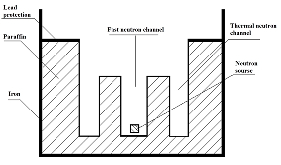
Figure 1. Block for producing thermal neutrons.
The next step of the research is to measure and determine the magnitude of the thermal neutron flux. The activation method is considered the simplest and most convenient method for this purpose. The manganese isotope 55Mn was used as a target detector. Its advantages as an activation detector of thermal neutrons are a large effective activation cross-section and a simple scheme for the decay of the artificial isotope. When measuring neutron fluxes of low intensity, the comparatively short half-life of the artificial radioactive isotope of manganese allows for measurements of the detectorʼs activity after short-term irradiation.
The thermal neutron flux density is determined by the expression:
|
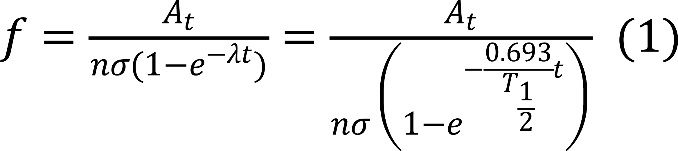
It should be noted that the effective activation cross-section of the manganese isotope 55Mn for thermal neutrons is 13.3 barns. The mass of the target detector was 10g.
In the second part of the work, an X-ray diffraction analysis of CdTe crystals obtained by the Bridgman method was carried out before and after irradiation with thermal neutrons, which are used in nuclear detectors with high radiation resistance. X-ray diffraction analysis of CdTe crystals was performed on a DRON-3.0 diffractometer (Figure 2).
|
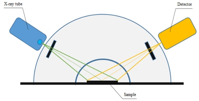
Figure 2. Scheme of X-ray diffraction analysis.
The instrumental error is checked by measuring X-ray pulses for 100s upon reflection of a powder sample of KP-3 (every hour in series of 11 measurements) for 6h.
The samples were studied in the range of angles from 20° to 50° in 2θ. The X-ray source operated with an emission current of 6mA, and the voltage between the cathode and anode in the X-ray tube was 36kV. Ordinary water was used to cool the anode. Since single crystals were used in the X-ray diffraction analysis, the maximum direction of X-ray diffraction is determined from the Wulf-Bragg condition:
|
The wavelength of the X-rays was 0.154nm.
2.2 Computer Calculations and Modeling
The structural, electronic and optical properties of CdTe are investigated based on density functional theory. Calculations were carried out in the VASP plane wave package[29]. For the first time, the crystal structures of the cubic phase were fully optimized taking into account the relaxation of lattice parameters and atomic positions.
To simulate the effect of irradiation on the properties of CdTe, a supercell consisting of 216 atoms (108 cadmium and 108 tellurium) was created. Then, one cadmium atom was removed from the supercell as the equivalent of a defect that appears after irradiation with a flux of thermal neutrons. Next, the structures were relaxed using the GGA functional[30]. After a series of convergence tests, the kinetic energy threshold was set at 450eV. The band gap values of the materials under study were also calculated and compared using the GGA exchange-correlation functional.
3 RESULTS AND DISCUSSION
3.1 Structural Properties of CdTe
Figure 3 shows the three-dimensional optimized structures of CdTe.
|
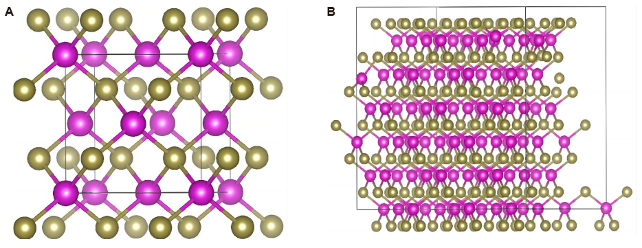
Figure 3. Three-dimensional optimized CdTe structures. A: initial cell; B modified cell Cd107Te108.
From Figure 3A it is clear that the initial CdTe cell has a cubic structure in the form of “zinc blende”. Cadmium atoms are located at the tops and faces of the crystal lattice. Tellurium atoms are located inside a crystal cell. As can be seen from the Figure 3, each cadmium atom is connected to four tellurium atoms. Figure 3B shows the structure of the modified cell of Cd107Te108, which consists of 107 cadmium atoms and 108 tellurium atoms. It is clear from the Figure 3 that one tellurium atom, after tearing out one cadmium atom, does not form a bond with the remaining atoms of the crystal cell. The released free atoms of cadmium and tellurium manifest themselves as defects in the crystal lattice and affect the structural and electrical parameters of the material.
Table 1 shows the results of calculations and experiments on measuring the parameters of the CdTe crystal lattice.
Table 1. Results of Calculations and Experiments for the Structural Parameters of CdTe
Parameter |
Original CdTe cell |
Modified cell Cd107Te108 |
Experiment |
α=β=γ, degree |
90.0 |
90.0082 |
90.0 |
a=b=c, Å |
6.51 |
6.50 |
6.50-6.36 |
V, Å3 |
275.79 |
275.19 |
274.625-257.259 |
Table 1 shows that the results of modeling and experiments[31] for the structural parameters of CdTe coincide. The calculation results show that after the removal of one cadmium atom from the Cd107Te108 structure, a decrease in the parameter a and the volume of the unit cell is observed. This trend can also be seen in the experimental results. The decrease in parameter a and the volume of the crystal cell of CdTe in the fourth column is associated with irradiation of the crystal with thermal neutrons.
Previously, the structure of CdTe crystals after irradiation with thermal neurons was studied experimentally. Since cadmium is a good absorber of thermal neutrons, the main nuclear reactions occur with this element. As a result, the number of cadmium atoms in the material decreases and new isotopes appear. Thus, the structure of the material changes, which is reflected in its X-ray patterns. It has been experimentally shown that in the region of low thermal neutron fluxes the reflections narrow and shift to small angles. Figure 4 compares the obtained X-ray diffraction patterns from the experiment and the X-ray diffraction patterns obtained from the optimized geometry using the REFLEX program included in the Materials Studio software package.
|
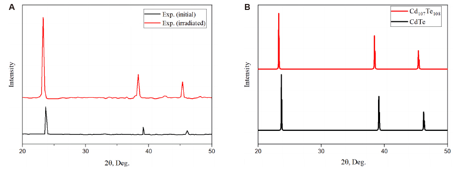
Figure 4. Results of X-ray diffraction analysis of CdTe. A: comparison of experimental X-ray patterns of unirradiated (top) and irradiated samples with a flow of 1.3∙108 n/cm2 (bottom); B: calculated X-ray diffraction patterns of the original CdTe and the modified Cd107Te108 cell.
The reflections that are observed in the X-ray diffraction pattern are the result of the reflection of X-rays from the (111), (220) and (311) crystal planes, respectively. Based on the results of quantum chemical calculations for CdTe, one can notice a change in the lattice parameter and interplanar distance, since the X-ray patterns show a shift of X-ray reflections towards small angles, which is in good agreement with previous experimental data[32]. The shift of X-ray reflections towards small angles occurs due to fluctuations in the electron density inside the material.
3.2 Electronic Properties of CdTe
The electronic properties of CdTe were assessed by the band gap shape, energy band distribution and other parameters. These parameters are important parameters of semiconductor crystals that are used to create photoconverting devices. Table 2 shows the values of the Fermi energy, the band gap of the unit cell and supercell of Cd107Te108.
Table 2. Quantum-chemical Parameters of the Unit Cell and Supercell of CdTe
Parameter |
Original CdTe cell |
Modified cell Cd107Te108 |
Fermi energy eV |
1.81 |
2.69 |
BG eV |
1.5 |
0.75 |
Total energy per unit cell |
4.80 |
4.76 |
Table 2 shows that when moving from the original cell to the modified cell, the band gap is halved. A decrease in the value of the total energy per unit cell is also observed.
The partial and total density of electronic states was calculated for the system of the original and modified Cd107Te108 cell (Figure 5). The calculated density of states of these systems is discussed from the point of view of the contribution of the s-, p-, d-states of the constituent atoms.
|
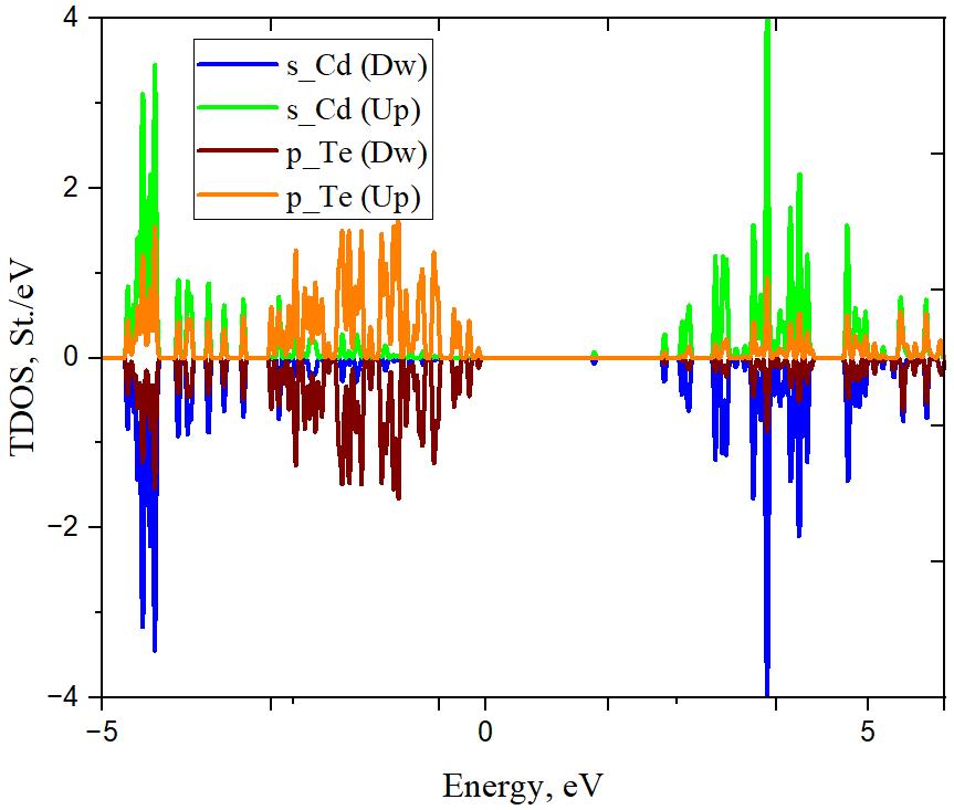
Figure 5. Density of electronic states of the original CdTe cell.
Analysis of the density of states of the initial CdTe cell shows that in the formation of electronic states of the VB in the energy range -5 to -3eV, the contribution of the s-states of the cadmium atom is significantly large. As one approaches the band gap, the contribution of the p-states of the tellurium atom increases. In the formation of electronic states of the CB in the energy range up to 5eV, the contribution of the s-states of the cadmium atom is very large, then the initiative to a small extent passes to the p-states of the tellurium atom. Figure 6 shows the density of electronic states of the modified Cd107Te108 cell.
|
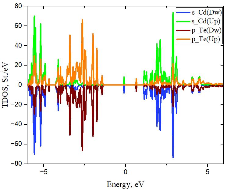
Figure 6. Density of electronic states of the modified Cd107Te108 cell.
It can be noted that the main contribution to the formation of electronic states of the modified Cd107Te108 cell in the VB region is made by the s-states of cadmium atoms and p-states of tellurium atoms. In contrast to the electronic states of the original cell, in this case the density of p-states of the tellurium atom is much higher. This indicates a decrease in the concentration of cadmium atoms in the material, as indicated by the experimental results.
In the band gap, due to the p-states of the tellurium atom, new electronic states appear, which lead to a decrease in the band gap. One can notice the predominant contribution of the s-states of cadmium atoms to the CB. Another important aspect is the sharp increase in the density of electronic states of Cd107Te108 relative to pure CdTe. It is usually assumed that an increase in the density of the state to increase the vacancy in the crystal, which in our case is justified by the appearance of defects after irradiation of CdTe with thermal neutrons. Such a phenomenon can be accompanied by an increase in the absorption capacity of the material, which is a very favourable effect.
3.3 Optical Properties of CdTe
In addition to the electronic properties, several optical parameters such as absorption coefficient, loss coefficient and photoconductivity of the crystals were also evaluated. The optical absorption band α (Figure 7A) of the original CdTe and modified Cd107Te108 begins at 0.1eV. For the original CdTe, the absorption band has a maximum at a photon energy of 3.9eV (emission wavelength 318nm), and for the modified Cd107Te108 the absorption maximum is observed at 2.6eV (emission wavelength 477nm). This means that the absorption band shifts from the ultraviolet region towards the visible part of the spectrum (more precisely blue) and the absorption coefficient increases by 20%. Further, a sharp decrease in the absorption coefficient is noticed at photon energies from 6 to 8eV for both crystals studied, since the density of electronic states decreases in this region.
|
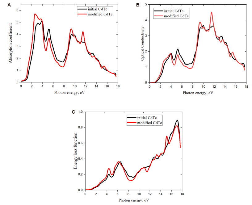
Figure 7. Optical characteristics of original CdTe and modified Cd107Te108. A: absorption; B: conductivity; C: energy loss coefficient.
In the photon energy range from 1 to 4eV, one can notice an improvement in the conductivity coefficient (Figure 7B) of the modified Cd107Te108. The listed changes make it possible to widely use these semiconductor crystals to create photoconverting devices.
In the photon energy range from 0.1 to 3eV, the loss coefficient (Figure 7C) of both structures has the same behavior. For high-energy photons, this parameter gradually increases. Calculations show that the influence of thermal neutrons has a positive effect on the optical properties of CdTe crystals. According to Figure 7, irradiation increases the absorption capacity and photoconductivity of CdTe in almost all energy ranges. In addition, the absorption peaks of CdTe after irradiation shifts towards lower energy, which indicates a decrease in the width of the forbidden zone and confirms the results given in Table 2.
4 CONCLUSION
The effect of the influence of small fluxes of thermal neutrons on changes in the geometry and electronic properties of CdTe has been studied. The changes occurring in the crystal structure were investigated by X-ray phase analysis, and the results were compared with data from quantum-chemical calculations. The results of quantum-chemical modeling of the process of interaction of thermal neutrons with CdTe crystals lead to a shift of peaks in the X-ray diffraction pattern of the samples, and also accompanies to a decrease in the width of the forbidden zone and a change in the electrical properties of the crystal. It is revealed that due to the occurrence of nuclear reactions of thermal neutrons with cadmium atoms the role of p-states of tellurium atoms in the formation of electronic states increases. The results of calculation of lattice parameters and width of the forbidden zone coincide with the experimentally calculated values. The results of calculations of optical parameters of CdTe showed that crystals irradiated with thermal neutrons are quite suitable for use in solar cells, since according to the results irradiation leads to an improvement in the optical characteristics of the material.
Acknowledgements
Not applicable.
Conflicts of Interest
The authors declared no conflicts of interest.
Author Contribution
Makhsudov B proposed the main ideas of the work and supervised the manuscript preparation process. Nematov D carried out quantum-chemical calculations, analyzed and interpreted the data. Yarov M carried out experimental studies, drawn tables, plotted graphs and wrote the paper.
Abbreviation List
BG, Bandgap
CB, Conduction band
CdTe, Cadmium telluride
VB, Valence band
References
[1] Romeo A, Artegiani E. CdTe-Based Thin Film Solar Cells: Past, Present and Future. Energies, 2021; 14: 1684.[DOI]
[2] Mauricio AF, Menéndez-Proupin E. Sn doped CdTe as candidate for intermediate-band solar cells: A first principles DFT+GW study. J Phys Conf Ser, 2016; 720: 012033.[DOI]
[3] Artegiani E, Gasparotto A, Meneghini M et al. How the selenium distribution in CdTe affects the carrier properties of CdSeTe/CdTe solar cells. Sol Energy, 2023; 260: 11-16.[DOI]
[4] Michael AS, McCandless B, Adam BP et al. CdTe-based thin film photovoltaics: Recent advances, current challenges and future prospects. Sol Energ Mat Sol C, 2023; 255: 112289.[DOI]
[5] Zghaibeh M, Okonkwo PC, Emori W et al. CdTe solar cells fabrication and examination techniques: A focused review. Int J Green Energy, 2023; 20: 5.[DOI]
[6] Paudel NR, Yan Y. Enhancing the photo-currents of CdTe thin-film solar cells in both short and long wavelength regions. Appl Phys Lett, 2014; 105: 18.[DOI]
[7] He X, Li C, Wu L et al. First-principles investigation on the electronic structures of CdSexS1-x and simulation of CdTe solar cell with a CdSexS1-x window layer by SCAPS. Rsc Adv, 2022; 12: 34.[DOI]
[8] Munshi A, Sampath W. CdTe Photovoltaics for Sustainable Electricity Generation. J Electron Mater, 2016; 45: 9.[DOI]
[9] Mehdi M, Ammari N, Merrouni AA et al. An experimental comparative analysis of different PV technologies performance including the influence of hot-arid climatic parameters: Toward a realistic yield assessment for desert locations. Renew Energy, 2023; 205: 695-716.[DOI]
[10] Shepidchenko A, Sanyal B, Klintenberg M et al. Small hole polaron in CdTe: Cd-vacancy revisited. Sci Rep, 2015; 5; 14509.[DOI]
[11] Kumar S, Kumar M, Pattabi M et al. Effect of Gamma Irradiation on Electrical Properties of CdTe/CdS Solar Cells. Mater Today, 2018; 5: 22570-22575.[DOI]
[12] Kondrik A. Degradation Mechanisms of the Detector Properties of CdTe and CdZnTe Under the Influence of Gamma Irradiation. East Eur J Phys, 2021; 3: 116-123.[DOI]
[13] Szeles C. CdZnTe and CdTe materials for X‐ray and gamma ray radiation detector applications. Phys Status Solidi B, 2004; 241: 783-790.[DOI]
[14] Bilenko DI, Galushka VV, Zharkova EA et al. The effect of low-dose gamma radiation on electrophysical properties of mesoporous silicon. Tech Phys Lett, 2017; 43: 166-168.[DOI]
[15] Belobrovaya O, Galushka B, Ismailova V et al. Influence of low doses of gamma radiation on optical properties of nanostructured silicon obtained by metal-stimulated in situ chemical etching [In Russian]. Izvestiya Saratov University, 2020; 20: 288-298.[DOI]
[16] Krylyuk S, Korbutyak D, Kryuchenko Y et al. Gamma-radiation effect on donor and acceptor states in CdTe and CdTe: Cl. J Alloys Compd, 2004; 371: 142-145.[DOI]
[17] Nasieka I, Boyko M, Strelchuk V et al. Gamma-irradiation effect on electron–phonon coupling in Ge-doped CdTe crystals: Raman and photoluminescence study. Solid State Commun, 2014; 196: 46-50.[DOI]
[18] Kamiński P, Żelazko J, Kozłowski R et al. Investigation of Energy Levels of Small Vacancy Clusters in Proton Irradiated Silicon by Laplace Photoinduced Transient Spectroscopy. Crystals, 2022; 12: 1703.[DOI]
[19] Haseman M, Somodi C, Stepanov P et al. Neutron irradiation induced defects in oxides and their impact on the oxide properties. J Appl Phys, 2021; 129: 21.[DOI]
[20] Gupta R, Chauhan R, Kumar R. Influence of gamma radiation on the optical, morphological, structural and electrical properties of electrodeposited lead selenide nanowires. Opt Mater, 2020; 99: 109538.[DOI]
[21] Bao L, Zha G, Zhang B et al. Investigation of neutron irradiation effects on the properties of Au/CdZnTe junction. Vacuum, 2019; 167: 340-343.[DOI]
[22] Makhsudov BI. Effect of thermal neutrons on the radiative characteristics of InGaAs/AlGaAs heterolasers. Quant Electron, 2015; 45: 216-217.[DOI]
[23] Makhsudov BI. Effect of gamma irradiation on the emissive characteristics of laser heterostructures. Quant Electron, 2012; 42: 745-746.[DOI]
[24] Sultonov N, Akobirova A, Khamrokulov R. Structural changes in single crystals of cadmium telluride upon irradiation with argon ions. Dushanbe, IA: Tajik National University; 2006.
[25] Sultonov N, Akobirova A, Azizov K et al. The structure and electrical properties of CdTe films. Dushanbe, IA: Tajik National University; 2011.
[26] Makhsudov BI, Akobirova AT, Brinkevich DI et al. Strength properties of neutrino-irradiated epitaxial CdTe films. Minsk, IA: Belarusian state University; 2018.
[27] Makhsudov BI. Neutron detector based on laser heterostructures DNGL-01. Russian RT patent No. 488, 2014.
[28] Makhsudov BI. Neutron detector based on InGaAs/AlGaAs heterolasers. Russian DAN RT, 2014.
[29] Nematov D. Analysis of the Optical Properties and Electronic Structure of Semiconductors of the Cu2NiXS4 (X = Si, Ge, Sn) Family as New Promising Materials for Optoelectronic Devices. J Opt Photonics Res, 2024; 1: 91-97.[DOI]
[30] Singh D. Electronic structure calculations with the Tran-Blaha modified Becke-Johnson density functional. Phys Rev B, 2010; 82: 20.[DOI]
[31] Nematov, D. Bandgap tuning and analysis of the electronic structure of the Cu2NiXS4 (X= Sn, Ge, Si) system: mBJ accuracy with DFT expense. Chem Inorg Mater, 2023; 1: 100001.[DOI]
[32] Nematov DD, Burhonzoda AS, Kholmurodov, KT, Lyubchyk, AI, & Lyubchyk, SI. A Detailed Comparative Analysis of the Structural Stability and Electron-Phonon Properties of ZrO2: Mechanisms of Water Adsorption on t-ZrO2 (101) and t-YSZ (101) Surfaces. Nanomaterials, 2023; 13: 2657.[DOI]
[33] Nematov D. Molecular and Dissociative Adsorption of H2O on ZrO2/YSZ Surfaces. Int J Innov Sci Mod Eng, 2023; 11: 1-7.[DOI]
[34] Nematov D. Analysis of the Optical Properties and Electronic Structure of Semiconductors of the Cu2NiXS4 (X= Si, Ge, Sn) Family as New Promising Materials for Optoelectronic Devices. J Opt Photonics Res, 2024; 1: 91–97.[DOI]
[35] Yarov MT. Influence of thermal neutron flux on the lattice constant of cadmium telluride single crystals [In Russian]. Polytechnic Bulletin, 2022; 58: 8-11.
[36] Makhsudov BI, Akobirova AT, Yarov MT. Effect of thermal neutron irradiation on electrophysical and structural characteristics of chlorine-doped CdTe [In Russian]. Bulletin of TNU, 2022; 1: 116-128.
Copyright © 2024 The Author(s). This open-access article is licensed under a Creative Commons Attribution 4.0 International License (https://creativecommons.org/licenses/by/4.0), which permits unrestricted use, sharing, adaptation, distribution, and reproduction in any medium, provided the original work is properly cited.


