High Photosensitivity Nanocrystalline p-Cu2S/n-FTO Heterojunction Photodetectors Prepared by Dip Coating Method
Madhavi Sharad Darekar1*, B M Praveen1
1Department of Nanotechnology, Institute of Engineering and Technology, Srinivas University, Mangalore, Karnataka, India
*Correspondence to: Madhavi Sharad Darekar, PhD (Physics), Post Doctoral Fellow, Department of Nanotechnology, Institute of Engineering and Technology, Srinivas University, Mukka, Surathkal, Mangalore 574146, Karnataka, India; Email: madhavi_darekar28@rediff.com
DOI: 10.53964/jmn.2023001
Abstract
Objective: The aim of present work is to fabricate nanocrystalline p-Cu2S/n-FTO heterojunction photo detectors with high photosensitivity.
Methods: Copper sulphide (Cu2S) is semiconductor compound belonging to I-VI group. Cost effective chemical method was used to synthesize thioglycerol capped Cu2S nanoparticles with improved optoelectronic and physical properties. These nanoparticles were investigated by ultraviolet-visible (UV-Vis) absorption spectroscopy, photoluminescence (PL) and transmission electron microscopy (TEM). Cu2S films were deposited on fluorine doped tin oxide (FTO) glass slides using cost effective dip coating method at different dip times and heat treated in air atmosphere. Wide band gap fluorine doped tin oxide, n-type semiconductor was used as transparent window material together with narrow band gap Cu2S, p-type semiconductor used as absorber layer in case of Cu2S/FTO heterojunction photo detectors under reverse biased mode and illumination.
Results: Cu2S films were characterized by X-ray Diffraction (XRD), Scanning Electron Microscopy (SEM), Energy Dispersive Analysis by X-rays (EDAX), Mapping and Atomic Force Microscopy (AFM). Selected Area Electron Diffraction (SAED) images showed ring patterns indicating that Cu2S nanoparticles are polycrystalline in nature and spot patterns indicating that Cu2S nanoparticles are monocrystalline in nature.
Conclusion: Previously, preparation of optoelectronic devices such as photo detectors using Cu2S films has not been reported. In this study, photo detectors having enhanced photosensitivity were prepared using Cu2S films. I-V characteristics of p-Cu2S/n-FTO heterojunctions under dark and illumination conditions were examined. It was observed that film conductivity decreases under dark condition and increases under illumination condition with increase in dip time in case of Cu2S/FTO heterojunction photo detectors.
Keywords: synthesis, characterization, nanoparticles, Cu2S thin films, photo detectors, dip coating method
1 INTRODUCTION
Cuprous sulphide (Cu2S) is an indirect band gap p-type semiconductor belonging to I-VI group with a bulk band gap of 1.21eV at room temperature[1]. Cu2S is a binary semiconducting material[2] which can be used in various applications such as photo sensor, catalyst[3], high temperature thermistors, ion conduction etc.[4]. Copper sulphide (Cu2S) can be used as an absorber material in photovoltaic (PV) applications due to its potential properties such as elemental abundance, p-type nature, high optical absorption coefficient in the visible region of solar spectrum (α>104cm-1) and environmental stability. So it was used in combination with fluorine doped tin oxide (FTO) in optoelectronic devices with special interest[5]. The five stable phases of Copper sulphide (Cu2S) (CuxS, where x=1 to 2) with different stoichiometry are Cu2S (chalcocite), Cu1.96S (djurleite), Cu1.8S (digenite), Cu1.75S (anilite) and CuS (Co-Vellite) at room temperature with varying morphologies and various unique optoelectronic properties[6].
The methods like dip coating[7], vacuum evaporation, chemical bath deposition, spray pyrolysis, solid state reaction, reactive magnetron sputtering, atomic layer deposition, co-evaporation, electro synthesis, chemical vapour deposition, modified chemical bath deposition, electrochemical, microwave assisted chemical bath deposition (MA-CBD), successive ionic layer adsorption and reaction (SILAR) etc. were used for the deposition of Cu2S thin films[8]. Due to simplicity, cost effective instrumentation, deposition of large area thin film, utility of same solution and availability of starting materials, Copper sulphide (Cu2S) thin films were deposited in a large amount by using the dip coating method as compared to the other techniques[7,9]. Also high pressure or vacuum was not needed during dip coating thin film deposition[2]. The parameters which affect the structural, optical and electrical properties of the dip coating deposited thin films are dip time and chemical reagents used in the dip coating method.
In the present study, the Cu2S nanoparticles prepared using the non-aqueous chemical method were analysed by UV-Vis Absorption Spectroscopy, PL and TEM and the dip coating deposited Cu2S thin films were investigated by XRD, SEM, EDAX, Mapping and AFM.
Photo-sensitivity is the way of quantifying the minimum amount of light needed to produce an electronic signal and is typically wavelength dependent. Photo detectors, also known as photo sensors are sensors of light or other electromagnetic radiation[10]. There is a wide variety of photo detectors which may be classified by mechanism of detection[11], such as photoelectric or photochemical effects, or by various performance metrics, such as spectral response i.e., the response of a photo detector as a function of photon frequency. Semiconductor-based photo detectors typically have a p-n junction that converts photons (or light) into electrical current[12]. The absorbed photons make electron-hole pairs in the depletion region. This mechanism is also known as the inner photoelectric effect. The P layer has an abundance of holes (positive), and the N layer has an abundance of electrons (negative). Photo diodes and photo transistors are a few examples of photo detectors. The package of a photodiode allows light (or infrared or ultraviolet radiation, or X-rays) to reach the sensitive part of the device. The package may include lenses or optical filters. Photo diodes usually have a slower response time as their surface area increases. A photo diode is designed to operate in reverse bias[13]. Photo diodes can be manufactured from a variety of materials including Silicon, Germanium, Lead (II) Sulphide, Mercury Cadmium Telluride, Indium Gallium Arsenide and Indium Gallium Arsenide Phosphide[14]. These materials are applicable in consumer electronics devices like smoke detectors, compact disc players, medical equipment and infrared (IR) remote control devices to control ACs and TVs. Each material uses different properties for cost benefits, increased sensitivity, wavelength range, low noise levels, or even response speed. The material used to make a photo diode is critical to defining its properties, because only photons with sufficient energy to excite electrons across the material’s bandgap will produce significant photocurrents. The photo diodes having the higher band gap generate less noise than the photo diodes having the lower band gap. Solar cells convert some of the light energy absorbed into electrical energy. A solar cell used to generate electric solar power is a large area photo diode.
Photo diodes are used in scientific and industrial instruments to measure light intensity, either for its own sake or as a measure of some other property (e.g., density of smoke). A photo diode can be used as the receiver of data encoded on an infrared beam, as in household remote controls. Photo diodes can be used to form an optocoupler, allowing transmission of signals between circuits without a direct metallic connection between them, allowing isolation from high voltage differences. Binary materials, such as MoS2, and graphene emerged as new materials for the production of photo diodes[15].
In the present work, the nanocrystalline p-Cu2S/n-FTO heterojunction photo detectors with high photosensitivity were fabricated and their I-V characteristics were examined under dark and illumination conditions.
2 MATERIALS AND METHODS
All the materials which may be metals, semiconductors or insulators have size dependent physic-chemical properties below a certain critical size. The critical size depends upon the composition and structure of the material. The critical size is below ~ 100nm for most of the materials[16]. At such a small size even the shape of the material and interactions between nanomaterials decide the properties of the material. Thus the materials have different properties just due to their size, shape or assembly. A large number of methods like chemical capping, sol-gel synthesis, sono-chemical synthesis, electro deposition, cluster deposition, use of zeolites, glass matrix, polymer coating have been used to synthesize nanometer-sized particles. The electrostatic interaction between the particles mainly controls the growth of the particles in solutions. These particles should be passivated using some surfactant or embedded in some solid matrix like polymer, zeolite or silica glass in order to prevent the coalescence of particles and keep their properties according to the size. The CdS semiconductor nanoparticles were synthesized by using the cost effective wet chemical method. The properties of the nanoparticles are often strongly dependent on the particle size, shape and surface properties which can be used to study the size quantization effect observed in semiconductor nanoparticles. Materials in the micrometer scale mostly exhibit the physical properties same as that of the bulk form. But, the materials in the nanometer scale exhibit the physical properties distinctively different from that of the bulk form[16].
The method for the synthesis of thioglycerol capped Cu2S nanoparticles (sample a) under nitrogen atmosphere is shown in Figure 1. The non-aqueous solutions of the analytical reagent (A.R.) grade chemicals like cuprous chloride (0.1M), thioglycerol (0.476M) and sodium sulphide (0.1M) were prepared by using ethyl alcohol (99% purity, Shandong S-sailing) and stirred in the reaction vessel by using a magnetic stirrer. The supernatant and the precipitate were separated and the precipitate was washed with acetone and diethyl ether and vacuum dried to obtain Cu2S nanoparticles with different sizes and energy gaps by changing the concentration of thioglycerol. All other parameters like the molarities of cuprous chloride, sodium sulphide, temperature, etc. which could alter the reaction product were kept constant. Thus the effect of only the capping agent was expected to be reflected. The thioglycerol concentration in sample ‘b’ is 0.238M and that in sample ‘c’ is 0.0428M.
|
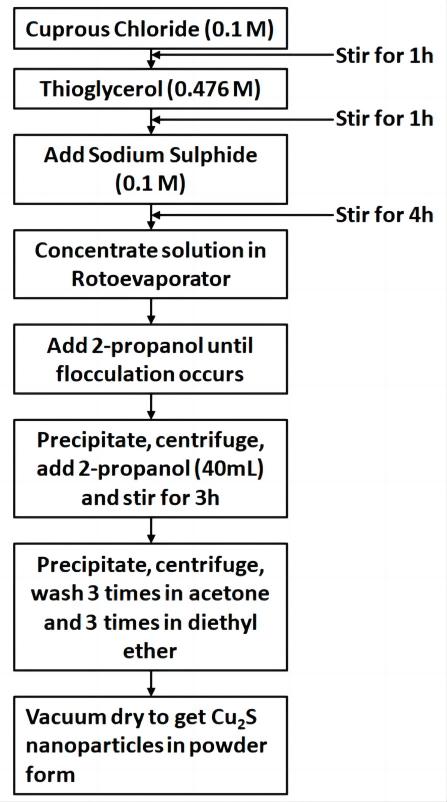
Figure 1. Method for the synthesis of Cu2S nanoparticles (sample a).
2.1 Preparation of Dip Coating Deposited Cu2S Films
Cu2S thin films approximately 19µm in thickness (sample a), 37µm in thickness (sample b) and 55µm in thickness (sample c) were deposited on the pre-cleaned transparent conducting oxide (TCO) like FTO glass substrates by using the dip coating technique for 3300 dip times, 6600 dip times and 9900 dip times respectively. These Cu2S films were heat treated in air atmosphere at 420°C for the improvement in their structural, electrical and optical properties and utilized for photo detector application. It has been reported that the structural, optical and physical properties of Cu2S films are changed by varying the dip time. An increase in dip time and film thickness decreases the transmission of the film and the optical energy gap and increases the grain size[2]. Due to this reason, the thickness of the p-type Cu2S layer was kept higher than the thickness of the n-type FTO layer in our study. Thin film thicknesses were experimentally measured by using laser profilometer.
The precursor solution prepared by dissolving copper acetate and thiourea in ethanol was used to deposit Cu2S nanocrystalline films on the precleaned glass substrates by the dip coating method. Cu2S samples were dissolved in distilled water to prepare the precursor solution which was used for the deposition of Cu2S thin films on the glass substrates by the expensive spin coating method[17]. In the present work, the Cu2S nanoparticle powders were dispersed in ethyl alcohol to prepare the precursor solutions. The dip coating method was used to deposit Cu2S thin films on the pre-cleaned FTO glass slides by using those most accurate precursor solutions.
2.2 Preparation of p-Cu2S/n-FTO Heterojunction Photodetector
The full device structure i.e., glass/FTO/Cu2S/Ag is shown in Figure 2. FTO electrode was used as the transparent front electrical contact (i.e., cathode) for the photo detector. The silver layer of approximately 265nm thick with low specific resistivity, good thermal stability and good adherence to substrate[18] was deposited on the Cu2S film (sample a) to form the back metal contact (i.e., anode) of the photo detector. Similarly, the back metal contacts (i.e., anodes) of the photo detectors were formed by deposition of the silver layersof approximately 515nm thick on the Cu2S film (sample b) and 766nm thick on the Cu2S film (sample c) respectively. The crystallinity of heat treated Cu2S films was increased and the band gaps and resistivities of those films were decreased. Similar observations have been made by More et al[3]. N-type FTO thin film with large band gap energy was used as the transparent window material and p-type Cu2S semiconductor with small band gap energy was used as the absorber material for low cost photo detectors. Three p-Cu2S/n-FTO heterojunction photo detectors were prepared by using three dip coating deposited Cu2S films (samples a, b and c).
|
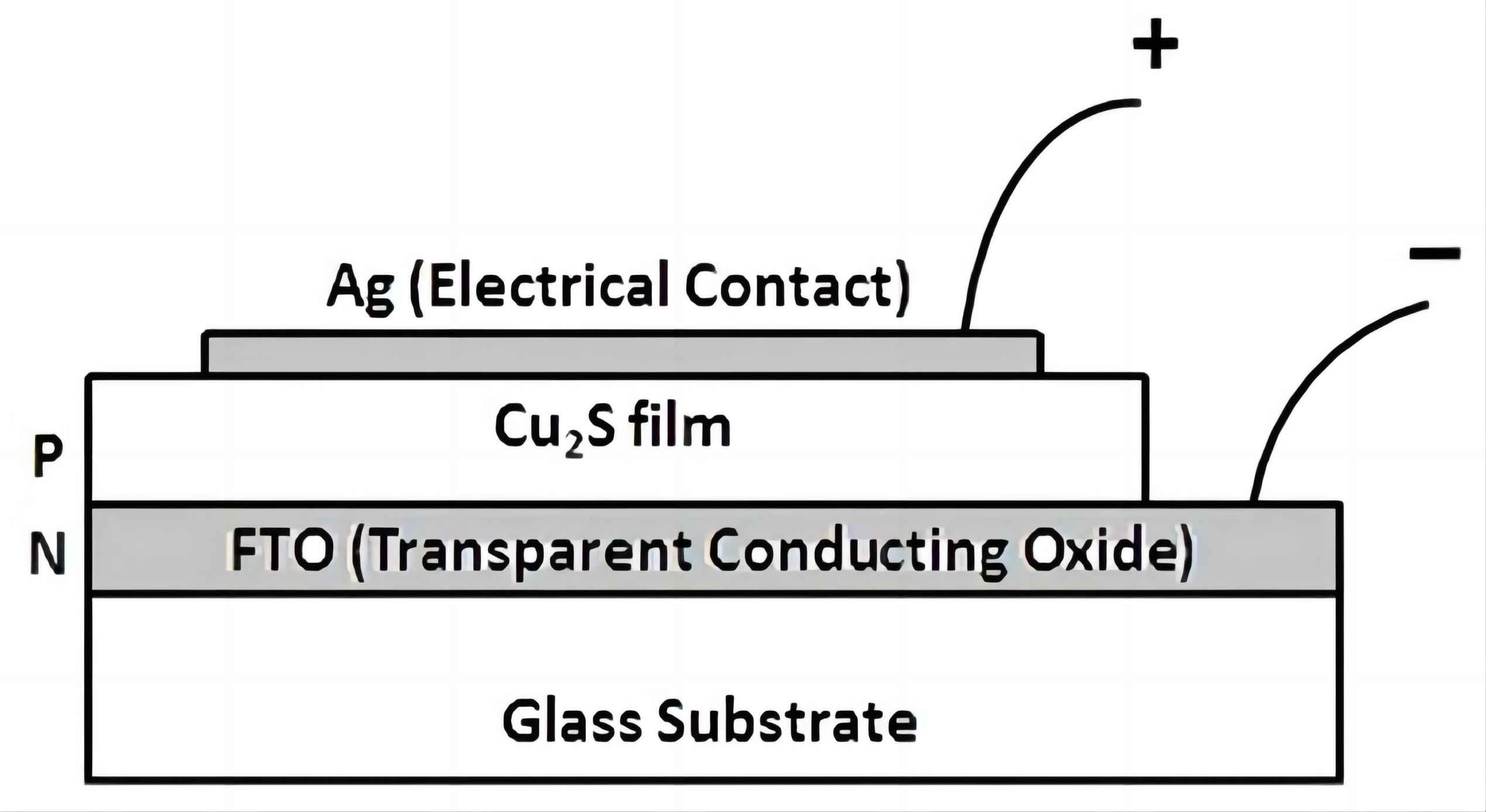
Figure 2. p-Cu2S/n-FTO heterojunction photo detector.
The forward currents of three p-Cu2S/n-FTO heterojunction photo detectors were measured with an increase in applied voltages under the effect of forward bias by using the digital multimeter. The photocurrents of these three photo detectors were measured with an increase in applied voltages under the effect of reverse bias by using the digital multimeter.
3 RESULTS AND DISCUSSION
3.1 Optical Studies
Figure 3 shows the plot of absorbance versus wavelength for the Cu2S nanoparticles of different sizes i.e., samples a, b and c obtained at room temperature by changing the concentration of thioglycerol. The thioglycerol concentration in sample ‘a’ is 0.476M, that in sample ‘b’ is 0.238M and that in sample ‘c’ is 0.0428M. The optical properties of Cu2S nanoparticles were studied by the absorbance measurements in the range 300-1200nm. The Cu2S samples prepared by dispersing the Cu2S nanoparticle powders in double distilled water were investigated by UV-Visible absorption spectroscopy.
|
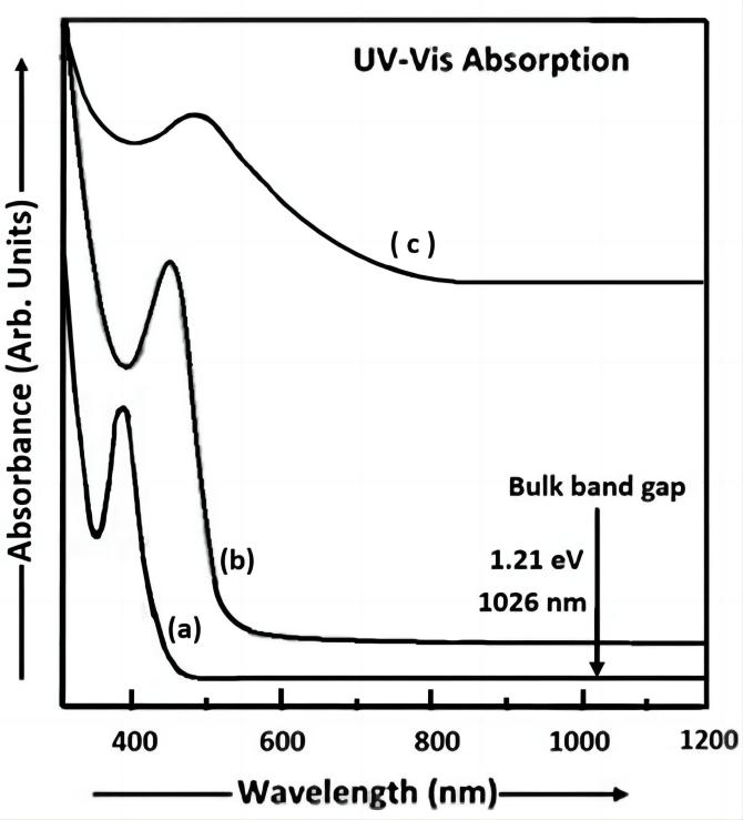
Figure 3. UV-Visible absorption spectra of Cu2S nanoparticles (samples a, b and c).
The equation of the energy of a photon, E=hv (Planck’s quantum theory of radiation)[19] was used to calculate the energy gap of the nanoparticles. The UV-Vis absorption spectrum of sample a shows the peak with higher absorption at 390nm (energy gap ~ 3.18eV) i.e., on the shorter wavelength side. The absorption spectrum of sample b shows the peak at 460nm (energy gap ~ 2.70ev) and the spectrum of sample c shows the peak with lower absorption at 490nm (energy gap ~ 2.53ev). Thus, the energy gap varies from 1.21ev to 3.18ev in Cu2S nanoparticles. From this discussion, it is concluded that there is an increase in energy gap with a decrease in particle size. Thus, the blue shift is observed in the optical absorption spectra of Cu2S nanoparticles (samples a, b and c). The estimated value of the particle size in sample a is 7.29nm, that in sample b is 8.65nm and that in sample c is 9.32nm.
The Cu2S material has narrow band gap (Eg ~ 1.21ev) at room temperature. Thus, from Figure 3, it can be clearly seen that the absorption peak shifts to the smaller wavelength with an increase in absorbance and thioglycerol concentration. This indicates the formation of nanoparticles. From Figure 3, it can be observed that the sharpness of the excitonic peak reduces with an increase in particle size and a decrease in energy gap. The size of Cu2S particles synthesized using the aqueous chemical method by Saraf[17] is higher than that of Cu2S particles synthesized in our study.
Figure 4 shows the photoluminescence spectra of Cu2S nanoparticles having various molarities of thioglycerol i.e., samples a, b and c. The thioglycerol concentration in sample a is higher than that in sample b and the thioglycerol concentration in sample b is greater than that in sample c.
|
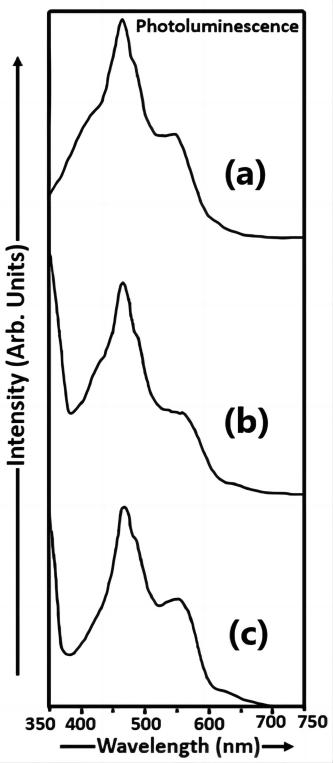
Figure 4. Photoluminescence spectra of Cu2S nanoparticles (samples a, b and c).
The electron transitions from various energy levels to lower energy levels are analysed by the PL technique[20]. The de-excitation process is due to direct recombination of the electron in the conduction band and the hole in the valence band giving rise to band edge luminescence. In such a situation it is expected that the excitation spectrum and the luminescence spectrum overlap at least partially. It is possible that the photo excited electron goes to the conduction band but on a scale of a few pico seconds it is transferred to a defect level. From this level it may radiatively recombine with a hole in the valence band or above it. When the luminescence takes place by recombination of electron trapped in some intermediate state between the valence band and the conduction band and a hole, then the luminescence wavelength would appear to be at longer wavelength corresponding to the lower energy of transition. If impurities or other electrically active defects are present, the electron levels within the band gap may be introduced, such as the donor and acceptor levels, except that they lie closer to the centre of the band gap. In case of lower concentration of thioglycerol defect levels may arise. These levels would be located below the conduction band. Light radiation of specific wavelengths may be emitted as a result of electron transitions involving these levels within the band gap.
The spectrum of sample c was recorded for an excitation wavelength of 335nm and the photoluminescence peak was observed at 468nm. Similarly, the spectrum of sample b was recorded for an excitation wavelength of 348nm and the PL peak was observed at 467nm. The spectrum of sample a was recorded for an excitation wavelength 293nm and the PL peak was observed at 468nm The intensity of the PL peak was increasing in sample c. Due to less concentration of thioglycerol in sample c, the increase in photoluminescence intensity is attributed to sulphur ion vacancies. Even if we increase the amount of thioglycerol in sample b still the luminescence intensity increases as thioglycerol does not totally cover the surfaces of the large sized Cu2S particles and the bonding between thioglycerol and Cu2S is reversible. In sample b, the enhancement in photoluminescence intensity is attributed to the sulphur ion vacancies. In sample a, the luminescence intensity is reduced due to the removal of sulphur ion vacancies by the capping agent which is thioglycerol. Thus from this discussion, it is concluded that in samples c, b and a, there is a quenching of the PL intensity with an increase in thioglycerol and a decrease in particle size. The addition of thioglycerol induces a slight blue-shift of the luminescence peak in sample b. Band-edge luminescence is not observed in all the three samples. The UV-Visible absorption peak is observed at 1026nm and the band gap (Eg) of bulk Cu2S material is 1.21ev at room temperature. Thus from Figure 4, it can be clearly seen that there is a blue shift in the PL emission spectra of Cu2S nanoparticles (samples a, b and c). The intensity of the emission peaks of Cu2S nanoparticles (samples a, b and c) synthesized in our study is higher than the intensity of the emission peaks of Cu2S nanoparticles synthesized using the aqueous chemical method by Gurnani et al[21].
3.2 Structural Investigation
Figure 5 shows the X-ray diffraction (XRD) spectra of Cu2S films deposited with different dip times (samples a, b and c) on FTO glass slides using the dip coating method at room temperature. The XRD analysis is used to study the phase formation in Cu2S films. The Cu2S particles have approximately the same average particle size. It shows that the diffraction patterns are similar for the various thioglycerol concentrations incorporated in Cu2S nanoparticles. The average size of the particles in sample a is 82.84nm, that in sample b is 82.8nm and that in sample c is 82.8nm. From these three values of average particle size, it is clearly seen that the crystallite size remains constant in Cu2S nanoparticles (samples a, b and c) with a slight difference in thioglycerol concentrations even if the dip time increases from sample a to sample c. The micro strain (ɛ) and dislocation density (δ) were estimated by using the given formulae, ![]() and
and ![]() [22]. The values of ɛ of Cu2S nanoparticles in samples a, b and c are 4.188×10⁻⁴m, 4.189×10⁻⁴m and 4.189×10⁻⁴m respectively and the values of δ of Cu2S nanoparticles in samples a, b and c are 1.457×10¹⁴ lines/m2, 1.458×10¹⁴ lines/m2 and 1.458×10¹⁴ lines/m2 respectively. The diffraction peaks having small widths are observed at 2θ= 31.660º, 2θ=32.360º, 2θ=39.720º and 2θ=49.960º in large sized Cu2S particles (sample a), at 2θ=31.660º, 2θ=32.200º, 2θ=39.600º and 2θ=49.960º in large sized Cu2S particles (sample b) and at 2θ=31.640º, 2θ=32.200º, 2θ=39.680º and 2θ=49.880º in large sized Cu2S particles (sample c) originating from the lattice planes (103), (006), (105) and (112) which are very close to those reported in JCPDS (Joint Committee on Powder Diffraction Standards) data for Cu2S. The observed results confirm the presence of hexagonal-wurtzite structure. The intensity of the diffraction peaks increases with an increase in dip time or film thickness. This change can be observed in the Cu2S film because of the random orientation of deposited atoms during the atomic condensation of film formation at lower dip time and the directed orientation of the polycrystalline grains at higher dip time[8]. This indicates that the dip coating deposited Cu2S films are well-crystallized[2]. The spectral range used in X-ray diffraction patterns of Cu2S nanoparticles was 5º to 80º. The value of average crystallite size of Cu2S thin films deposited by the dip coating method in the present study is smaller than that (84nm) of Cu2S nanoparticles prepared using the aqueous chemical method by Saraf R[17].
[22]. The values of ɛ of Cu2S nanoparticles in samples a, b and c are 4.188×10⁻⁴m, 4.189×10⁻⁴m and 4.189×10⁻⁴m respectively and the values of δ of Cu2S nanoparticles in samples a, b and c are 1.457×10¹⁴ lines/m2, 1.458×10¹⁴ lines/m2 and 1.458×10¹⁴ lines/m2 respectively. The diffraction peaks having small widths are observed at 2θ= 31.660º, 2θ=32.360º, 2θ=39.720º and 2θ=49.960º in large sized Cu2S particles (sample a), at 2θ=31.660º, 2θ=32.200º, 2θ=39.600º and 2θ=49.960º in large sized Cu2S particles (sample b) and at 2θ=31.640º, 2θ=32.200º, 2θ=39.680º and 2θ=49.880º in large sized Cu2S particles (sample c) originating from the lattice planes (103), (006), (105) and (112) which are very close to those reported in JCPDS (Joint Committee on Powder Diffraction Standards) data for Cu2S. The observed results confirm the presence of hexagonal-wurtzite structure. The intensity of the diffraction peaks increases with an increase in dip time or film thickness. This change can be observed in the Cu2S film because of the random orientation of deposited atoms during the atomic condensation of film formation at lower dip time and the directed orientation of the polycrystalline grains at higher dip time[8]. This indicates that the dip coating deposited Cu2S films are well-crystallized[2]. The spectral range used in X-ray diffraction patterns of Cu2S nanoparticles was 5º to 80º. The value of average crystallite size of Cu2S thin films deposited by the dip coating method in the present study is smaller than that (84nm) of Cu2S nanoparticles prepared using the aqueous chemical method by Saraf R[17].
|
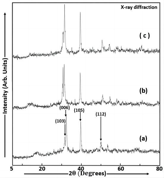
Figure 5. X-ray diffraction patterns of Cu2S films (samples a, b and c).
3.3 Morphological Investigation
A complete study of surface morphology examined by SEM images of Cu2S films (samples a, b and c) is shown in Figure 6 at a magnification of 50,000x. In sample a, the small sized Cu2S particles are obtained due to higher concentration of thioglycerol which is 0.476M. In sample b, the large sized Cu2S particles are obtained due to lower concentration of thioglycerol which is 0.238M. In sample c, the Cu2S particles having size larger than that of sample b are obtained due to lowest concentration of thioglycerol which is 0.0428M. From these three values of thioglycerol concentration it is clear that the particle size decreases with an increase in thioglycerol concentration. Cauliflower-like Cu2S particles are observed in samples a, b and c having different particle sizes. The shape of the particles is same but their sizes are different in samples a, b and c having various molarities of thioglycerol.
|
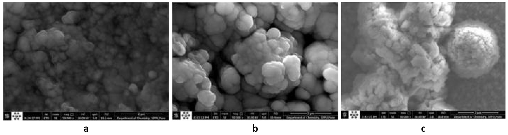
Figure 6. SEM images of Cu2S films (samples a, b and c) with magnification of 50,000. Scale bar: 2µm.
The large sized grains are observed in the Cu2S films prepared with the highest dip time which are shown in SEM micrographs (Figure 6). The surfaces of Cu2S films show the micron-sized large agglomerations which consist of many smaller grains of the size of a few tens of nanometres[23]. This indicates that the Cu2S films are nanostructured materials. The fine particles are observed on the surfaces of Cu2S films with a change in cluster size. The large grains of the size in the 45-306nm range were produced in Cu2S films after heat treatment in air atmosphere and the crystal defects in Cu2S films were reduced as shown in Figure 6. Thus, the average particle sizes obtained from the SEM analysis are higher than those determined from the XRD analysis due to the coalescence of newly produced crystal nuclei. Heat treatment in air changes the optical properties of the Cu2S films[4]. The cauliflower-like grains observed in the Cu2S films consist of polycrystalline Cu2S nanoparticles. The grains comprised of Cu2S nanoparticles with hexagonal morphology. The clusters were produced by coagulation of the polycrystalline Cu2S nanoparticles and the crystallite size increased by increasing the annealing temperature. The crystallinity can be improved by the heat treatment in air atmosphere[23]. The SEM images of dip coating deposited Cu2S thin films have high quality which is confirmed by the fine-grained nanostructures without micro cracks or pin holes. Similar observations were found by Rafea and associates[7].
The clusters consisting of numerous agglomerated spherical shaped nanosized particles were observed in the SEM images of Cu2S films deposited by chemical bath deposition on the glass substrates by Ismail et al.[2] and their number enhanced by increasing the deposition time.
The cross sections can be examined with high magnification by SEM. The material grain sizes can be determined and the layer thicknesses can be estimated by SEM. The uniformity of large area material coverage can be checked and the presence of various surface defects can be detected by SEM study[20]. The clusters of irregular large sized particles were observed on the surfaces of Cu2S films deposited by chemical bath deposition on the glass substrates. The large sized particles consisting of many agglomerated nanosized particles of spherical shape were observed in the SEM micrographs of CBD deposited Cu2S films by Ismail et al.[2] the number of clusters increased and the film uniformity decreased with an increase in deposition time.
The TEM images and the selected area electron diffraction (SAED) patterns of columnar shaped Cu2S nanoparticles (samples a, b and c) of different sizes are shown in Figure 7A and B. The magnification of the TEM images of Cu2S nanoparticles is 200nm. The small grains were observed on the Cu2S layers, but the size of these grains increased up to 306nm having columnar shape after heat treatment in air atmosphere. From Figure 7A (a-c), it is clearly seen that the particle size increases with a decrease in thioglycerol concentration and an increase in dip time and film thickness. The rings corresponding to the indexed planes (103), (006), (105), (112) indicate the polycrystalline nature of Cu2S nanoparticles which is shown in SAED images [Figure 7B (a-c)]. Also from Figure 7A (d-i), it is clearly seen that the particle size decreases with an increase in thioglycerol concentration and a decrease in dip time and film thickness. The SAED images of Cu2S nanoparticles [Figure 7B (d-i)] show the ring patterns indicating that all six Cu2S samples are polycrystalline. Figure 7A (j) shows the TEM image of Cu2S nanoparticles (sample j) and Figure 7B (j) shows the SAED pattern of Cu2S nanoparticles (sample j). The columnar shaped Cu2S particles were observed at 200nm. SAED is the diffraction pattern obtained in the reverse space of the lattice planes. The SAED image of Cu2S nanoparticles (sample j) shows the spot pattern indicating that this Cu2S sample is monocrystalline. The spot pattern also represents the XRD patterns and it is used to calculate the dB, the spacing between the lattice planes of a material. The spot pattern is more accurate and standard/fundamental technique which is used to find out the crystallographic information of any material. The brighter spots indicate an increase in crystallinity of the Cu2S sample.
|
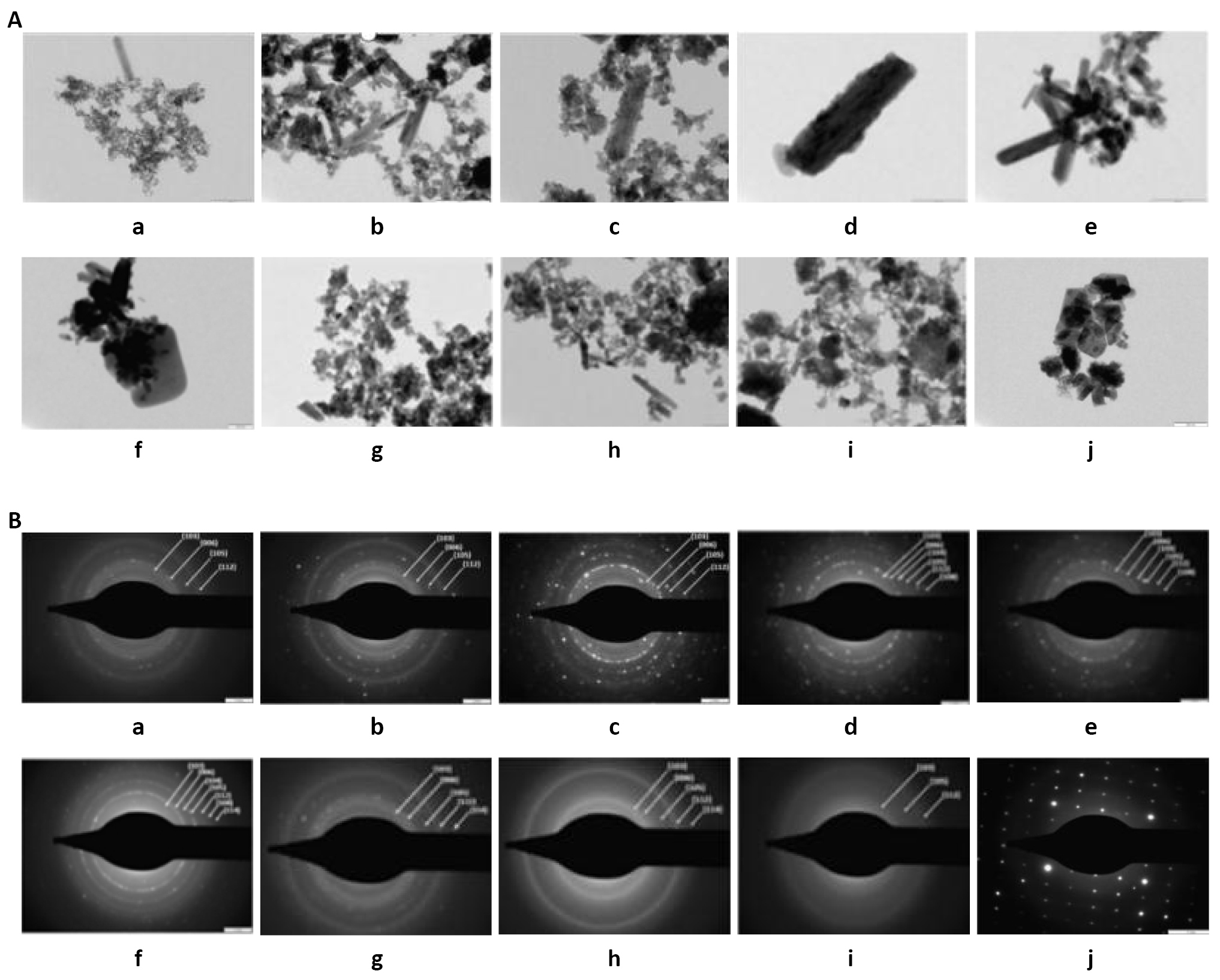
Figure 7. The TEM images and SAED patterns of Cu2S nanoparticles. A: TEM image of Cu2S nanoparticles (samples a, b, c, d, e, f, g, h, i, and j) with magnification of 200nm; B: SAED patterns of Cu2S nanoparticles (samples a, b, c, d, e, f, g, h, i, and j).
The optical and electrical properties of the films depend on their surface properties and this is a very important factor in the fabrication of optoelectronic devices[16]. For this reason, the surface topology of the Cu2S thin films was analysed by AFM study. The effect of dip time and heat treatment in air atmosphere on the surface morphology of the Cu2S films (samples a, b and c) was investigated by AFM analysis. Figure 8A illustrates the 2D-AFM images and Figure 8B illustrates the 3D-AFM images of Cu2S thin films deposited at different dip times. There is an increase in particle size and a decrease in film uniformity with an increase in dip time. Similar findings were observed by Ismail et al[2]. The 2D-AFM images indicate that the Cu2S films are characterized by highly dense spherical grains with modification in grain boundaries due to increase in surface roughness[5] and hills and valleys are observed in 3D-AFM images of Cu2S films. The size of the Cu2S clusters varies from 66-182nm at different magnifications. The average size of the Cu2S material grains shown in Figure 8B (a) is 66.47nm, that of Cu2S grains shown in Figure 8B (b) is 89.70nm and that of Cu2S grains shown in Figure 8B (c) is 142.8nm. The well-dispersed and highly dense nanospheres having approximately 30nm root-mean-square-roughness were observed in the AFM image of Cu2S thin film deposited by the dip coating technique by Rafea et al[7]. The 3D-AFM images observed by Ismail et al.[2] show the presence of irregular and large sized particles in the CBD deposited Cu2S films at higher deposition times.
|
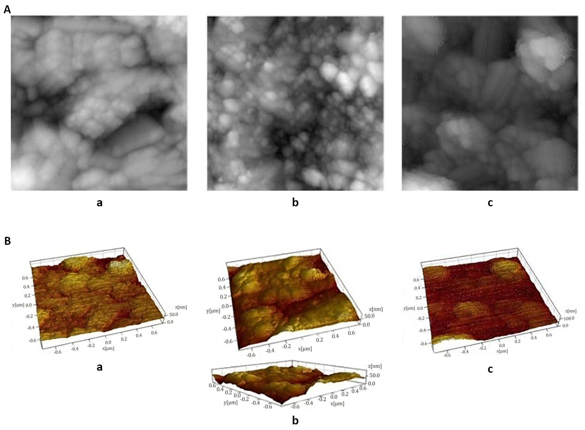
Figure 8. AFM images. A: 2D-AFM images of Cu2S films (samples a, b and c); B: 3D-AFM images of Cu2S films (samples a, b and c) with magnification of 1.5µm.
3.4 Compositional Investigation
The EDAX spectra were used for the compositional investigation obtained from the dip coating deposited Cu2S films (samples a, b and c) shown in Figure 9 respectively. The peaks of the elements like copper (Cu), sulphur (S), carbon (C), oxygen (O), chlorine (Cl), tin (Sn) and lead (Pb) observed in the EDAX spectrum of sample a show the elemental presence in atomic percentage in Table 1. The peaks of the elements like copper (Cu), sulphur (S), carbon (C), oxygen (O), chlorine (Cl), indium (In), tin (Sn), platinum (Pt), sodium (Na), tellurium (Te) and lead (Pb) observed in the EDAX spectrum of sample b show the elemental presence in atomic percentage in Table 2. The peaks of the elements like copper (Cu), sulphur (S), carbon (C), oxygen (O), sodium (Na), rhodium (Rh), chlorine (Cl), iron (Fe), indium (In), tin (Sn), tellurium (Te), platinum (Pt), lead (Pb) and nitrogen (N) observed in the EDAX spectrum of sample c show the elemental presence in atomic percentage in Table 3. The EDAX analysis of Cu2S thin films indicates the presence of copper and sulphur elements in samples a, b and c.
The stoichiometric atomic percentage ratios (Cu2S) of copper and sulphur elements for samples a, b and c are 2.01, 2.02 and 2.03 respectively. Thus it is concluded that the Cu2S thin films (samples a, b and c) have nearly perfect stoichiometry. The elemental analysis of Cu2S thin films (samples a, b and c) shows that there is a change in stoichiometric atomic percentage with various dip times. The two peaks having maximum intensity might have been transmitted from the Cu2S film (sample c) which is shown in the EDAX spectrum (Figure 9). This means that the composition of the deposited films depends on the dip time and film thickness[21]. The elements like copper (Cu), sulphur (S), magnesium (Mg), silicon (Si), sodium (Na), chlorine (Cl), oxygen (O), potassium (K), calcium (Ca) and nickel (Ni) were observed in the EDAX spectra of CBD deposited Cu2S films by Ismail et al[2].
|
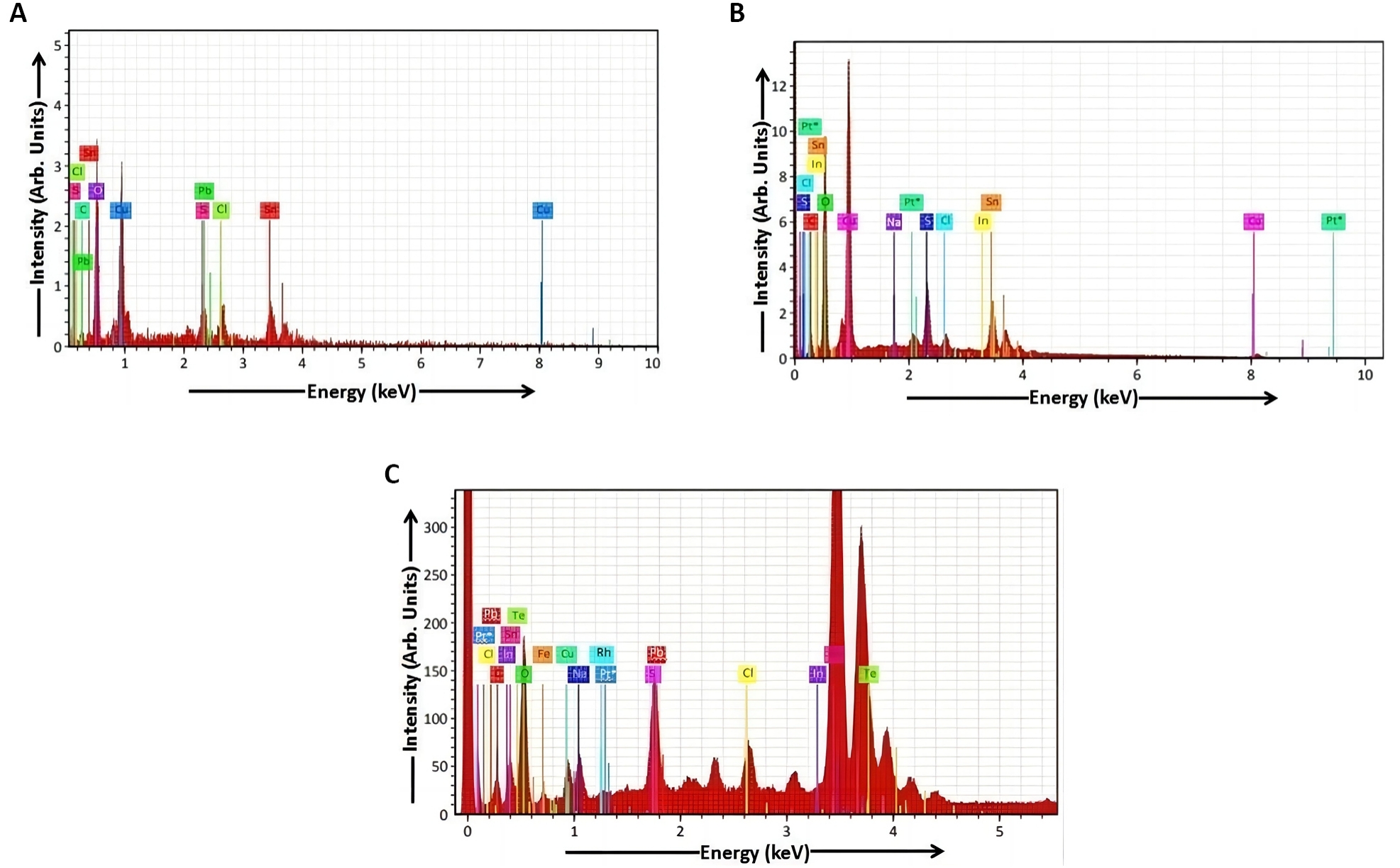
Figure 9. EDAX spectrum of Cu2S film. A: Sample a; B: Sample b; C: Sample c.
Table 1. EDAX Data of Cu2S Film (Sample a)
Element |
At. No. |
Netto |
Mass [%] |
Mass Norm [%] |
Atom [%] |
Abs. Error [%] (1 Sigma) |
Rel. Error [%] (1 Sigma) |
Carbon |
6 |
0 |
0.00 |
0.00 |
0.00 |
0.00 |
10.00 |
Oxygen |
8 |
1691 |
25.73 |
28.36 |
55.08 |
5.10 |
19.82 |
Sulphur |
16 |
308 |
1.81 |
2.00 |
10.99 |
0.16 |
8.98 |
Chlorine |
17 |
511 |
3.78 |
4.16 |
4.23 |
0.26 |
6.94 |
Copper |
29 |
1832 |
35.38 |
38.99 |
22.10 |
6.87 |
19.42 |
Tin |
50 |
1046 |
20.94 |
23.07 |
7.00 |
1.07 |
5.10 |
Lead |
82 |
255 |
3.11 |
3.42 |
0.60 |
0.28 |
8.93 |
Sum |
|
|
90.75 |
100.00 |
100.00 |
|
|
Table 2. EDAX Data of Cu2S Film (Sample b)
Element |
At. No. |
Netto |
Mass [%] |
Mass Norm [%] |
Atom [%] |
Abs. error [%] (1 Sigma) |
Rel. Error [%] (1 Sigma) |
Carbon |
6 |
2883 |
1.74 |
1.77 |
6.04 |
0.33 |
18.89 |
Oxygen |
8 |
56987 |
19.37 |
19.76 |
41.54 |
2.29 |
11.80 |
Sulphur |
16 |
19535 |
3.42 |
3.49 |
13.48 |
0.15 |
4.42 |
Chlorine |
17 |
6560 |
1.37 |
1.39 |
1.61 |
0.08 |
5.61 |
Copper |
29 |
99112 |
41.46 |
42.29 |
27.24 |
4.70 |
11.33 |
Indium |
49 |
5168 |
2.28 |
2.33 |
0.83 |
0.11 |
4.83 |
Tin |
50 |
39480 |
19.27 |
19.65 |
6.78 |
0.67 |
3.49 |
Platinum |
78 |
7317 |
0.00 |
0.00 |
0.00 |
0.00 |
1.78 |
Sodium |
11 |
406 |
0.08 |
0.08 |
0.12 |
0.03 |
37.70 |
Tellurium |
52 |
7007 |
4.27 |
4.36 |
1.40 |
0.18 |
4.24 |
Lead |
82 |
13184 |
4.77 |
4.87 |
0.96 |
0.20 |
4.26 |
Sum |
|
|
98.03 |
100.00 |
100.00 |
|
|
Table 3. EDAX Data of Cu2S Film (Sample c)
Element |
At. No. |
Netto |
Mass [%] |
Mass Norm [%] |
Atom [%] |
Abs. Error [%] (1 Sigma) |
Rel. Error [%] (1 Sigma) |
Carbon |
6 |
232 |
0.20 |
0.13 |
6.87 |
0.10 |
48.66 |
Oxygen |
8 |
9008 |
8.14 |
5.37 |
14.66 |
1.18 |
14.52 |
Sodium |
11 |
1595 |
0.88 |
0.58 |
0.99 |
0.09 |
9.92 |
Rhodium |
45 |
15967 |
5.88 |
4.49 |
1.60 |
0.33 |
5.63 |
Sulphur |
16 |
6832 |
3.14 |
2.07 |
15.75 |
0.16 |
5.19 |
Chlorine |
17 |
4746 |
2.11 |
1.39 |
11.99 |
0.11 |
5.08 |
Iron |
26 |
838 |
2.88 |
1.90 |
0.58 |
0.21 |
7.20 |
Copper |
29 |
915 |
1.25 |
0.83 |
31.99 |
0.32 |
25.22 |
Indium |
49 |
9900 |
9.33 |
6.16 |
1.08 |
0.35 |
3.80 |
Tin |
50 |
90510 |
90.31 |
58.40 |
9.27 |
3.19 |
3.35 |
Tellurium |
52 |
18895 |
24.05 |
16.45 |
1.80 |
0.89 |
3.55 |
Platinum |
78 |
562 |
0.00 |
0.00 |
0.00 |
0.00 |
1.78 |
Lead |
82 |
2945 |
2.03 |
1.33 |
2.87 |
0.12 |
6.05 |
Nitrogen |
7 |
1417 |
1.36 |
0.90 |
0.55 |
0.31 |
22.47 |
Sum |
|
|
151.56 |
100.00 |
100.00 |
|
|
3.5 Electrical Studies
From Figure 10, it is clearly seen that there is a decrease in forward current with an increase in dip time. The external potential difference was applied across the terminals of Cu2S/FTO heterojunction photo detector shown in Figure 2 under the forward biased mode. This means that the positive terminal of the external battery was connected to the P-region (i.e., Cu2S film) and the negative terminal of the external battery was connected to the N-region (i.e., FTO film) of Cu2S/FTO heterojunction. In forward bias, the applied electric field by the voltage source is in opposite direction to that of the built-in electric field in the depletion region. The net electric field is weakened, thus reducing the potential barrier and the width of the depletion layer to the diffusion of majority charge carriers from one side of the junction to the other. This results in domination of diffusion current (forward current) over the recombination current. The majority charge carriers are supplied from the external circuit, hence resulting in a net current flows under forward bias. When a forward voltage is applied across the terminals of Cu2S/FTO heterojunction photo detector, the forward current would flow easily through the photo detector from the P-side to the N-side. The potential barrier voltage is usually small. The forward voltage across the terminals of the photo detector is only a few tenths of a volt. Hence, the large current flows through the junction at small voltages. The direction of current gives the forward direction of P-N heterojunction. The current range is usually mA. The Cu2S film thickness increases from sample a to sample c. Hence the particle size (7.29nm) in sample a is smaller than that (8.65nm) in sample b and the particle size in sample b is smaller than that (9.32nm) in sample c. So the energy gap (3.18ev) of Cu2S nanoparticles in sample a is higher than that (2.70ev) of Cu2S nanoparticles in sample b and the energy gap of Cu2S nanoparticles in sample b is higher than that (2.53ev) of Cu2S nanoparticles in sample c. As the energy gap of P-region in sample a is high, a small amount of electron-hole pairs is produced. This means that the small amount of minority charge carriers (i.e., electrons in conduction band of P-region) and the large amount of majority charge carriers (i.e., holes in valence band of P-region and holes from positive terminal of battery) are produced in P-side of sample a. The optical band gap of FTO film is 3.80ev[24]. As the energy gap of FTO film is high, the small amount of minority charge carriers (i.e., holes in valence band of N-region) and the large amount of majority charge carriers (i.e., electrons in conduction band of N-region and electrons from negative terminal of battery) are produced in N-side. The large amount of majority charge carriers (i.e., the electrons in N-region and the holes in P-region) tend to diffuse from N-side to P-side and from P-side to N-side respectively and a large magnitude of forward current flows through the heterojunction. Thus, the energy gap and forward current decrease by the heat treatment in air atmosphere and also with an increase in dip time, film resistance, film thickness and particle size under dark condition. The values of the forward current of p-Cu2S/n-FTO heterojunction photo detector obtained in our study are higher than those of p-Cu2S/n-Si photo detector observed by Ismail et al[2].
|
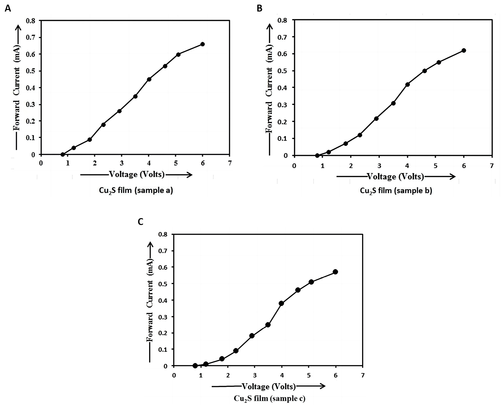
Figure 10. I-V characteristics of Cu2S/FTO heterojunction in dark condition. A: I-V characteristics of Cu2S/FTO heterojunction prepared using sample a at 3300 dip times in dark condition; B: I-V characteristics of Cu2S/FTO heterojunction prepared using sample b at 6600 dip times in dark condition; C: I-V characteristics of Cu2S/FTO heterojunction prepared using sample c at 9900 dip times in dark condition.
From Figure 11, it is observed that there is an increase in photo current with an increase in dip time. The external potential difference was applied across the terminals of Cu2S/FTO heterojunction photo detector shown in Figure 2 under the reverse biased mode. This means that the positive terminal of the external battery was connected to the N-region (i.e., FTO film) and the negative terminal of the external battery was connected to the P-region (i.e., Cu2S film) of Cu2S/FTO heterojunction. In reverse bias, the applied electric field by the voltage source is in same direction as that of the built-in electric field in the depletion region. The net electric field is strengthened, thus increasing the potential barrier and the width of the depletion layer. Under the reverse biased mode, the electrons in N-region and holes in P-region move away from the junction. The higher electric field reduces the probability that the majority charge carriers can diffuse across the heterojunction, hence the diffusion current decreases. The reverse current (photocurrent) which is due to the movement of minority free electrons in P-region and minority free holes in N-region across the junction flows in the circuit under reverse bias.
|
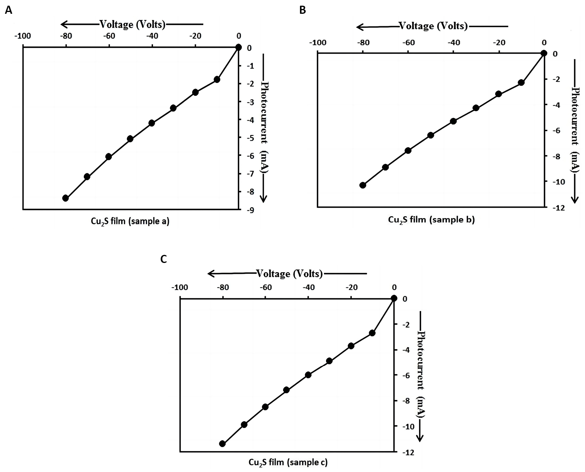
Figure 11. I-V characteristics of Cu2S/FTO heterojunctionunder illumination. A: I-V characteristics of Cu2S/FTO heterojunction prepared using sample a at 3300 dip times under illumination; B: I-V characteristics of Cu2S/FTO heterojunction prepared using sample b at 6600 dip times under illumination; C: I-V characteristics of Cu2S/FTO heterojunction prepared using sample c at 9900 dip times under illumination.
The intensity of the halogen light is 100mW/cm2. This light is incident on the non-conducting side of FTO glass slide. The thickness of the Cu2S layer should be high and that of FTO layer should be small. FTO film has high optical transparency (T≥85%)[7]. As the energy of halogen light was smaller than the energy gaps of the glass slide and FTO layer, the halogen light could be transmitted through the glass slide and FTO layer and reached the absorber layer (i.e., the Cu2S layer). As the energy of halogen light was higher than the energy gap of Cu2S nanoparticles, the maximum amount of halogen light could be absorbed by the Cu2S layer and a large amount of photo-generated charge carriers could be produced. Thus, a large magnitude of photocurrent could be generated. Thus it helped to enhance photosensitivity of the photo detector.
As the Cu2S film thickness increases from sample a to sample c, the particle size also increases and the energy gap decreases from sample a to sample c with an increase in dip time. As the energy gap of Cu2S nanoparticles in sample c is lesser than that of Cu2S nanoparticles in samples a and b, a large amount of photo-generated charge carriers are produced in the Cu2S layer of sample c. Hence, a large magnitude of photocurrent flows through Cu2S/FTO heterojunction. Thus, the photosensitivity increases and the energy gap decreases by the annealing temperature and also with an increase in dip time, film thickness and particle size under illumination condition. The total current through the photo diode is the sum of the dark current (current that is generated in the absence of light) and the photocurrent, so the dark current must be minimized to maximize the sensitivity of the device[25]. The photocurrent is linearly proportional to the irradiance to first order, for a given spectral distribution[26]. The values of the photo current of p-Cu2S/n-FTO heterojunction photo detector obtained in our study are higher than those of p-Cu2S/n-Si photo detector observed by Ismail et al[2].
The characterization results clearly showed that the high photosensitivity and cost favourable p-Cu2S/n-FTO heterojunction photo detectors were prepared at the different dip times and can be used for many applications.In the present study, a significant improvement was achieved in the photocurrent of p-Cu2S/n-FTO heterojunction photo detectors prepared using Cu2S films by the dip coating method due to low cost and simple, better results etc. under illumination condition. These photo detectors worked as forward biased P-N junction diodes under dark condition.
4 CONCLUSION
In summary, the non-aqueous chemical method was used to synthesize Cu2S nanoparticles. Cu2S films were successfully deposited on FTO glass substrates by using the dip coating method and heat treated in air at 420oC to improve their structural, optical and physical properties. Dip coating method has proven to be simple and cost effective and the deposition of large area thin films was achieved by this method. Cu2S nanoparticles and their films were analyzed using various characterization techniques. Blue shift was observed in UV-Visible absorption spectra of Cu2S nanoparticles having good optical properties. XRD analysis demonstrated that Cu2S nanoparticles have hexagonal single phase (wurtzite). TEM images of Cu2S nanoparticles demonstrated the columnar shaped particles with different sizes at high magnifications and an increase in particle size with an increase in dip time and film thickness. The SAED images of Cu2S nanoparticles demonstrated ring patterns indicating the polycrystalline nature of the particles and also bright spots indicating the monocrystalline nature of the particles. SEM images of Cu2S films demonstrated the Cauliflower-like particles with different particle sizes having various molarities of thioglycerol. The EDAX analysis of Cu2S thin films showed that the stoichiometric atomic percentage ratios of copper and sulphur elements in Cu2S samples a, b and c were 2.01, 2.02 and 2.03 respectively. Thus, it is clearly seen that the stoichiometry of Cu2S thin films is nearly perfect. 2D AFM images demonstrated the highly dense spherical grains in Cu2S films. 3D AFM images demonstrated the hills and valleys in Cu2S films. The p-Cu2S/n-FTO heterojunction photo detectors having high photosensitivity and low cost were prepared using Cu2S films and FTO glass substrates under illumination condition. FTO films showed high light transmission in the visible region of the electromagnetic spectrum due to which they were used as window layers in p-Cu2S/n-FTO heterojunction photo detectors. Cu2S films showed high light absorption in the visible region, thus making it possible to use them as absorber layers in photo detectors. It was observed that the photocurrent increases with an increase in dip time in case of illumination condition. The p-Cu2S/n-FTO heterojunction photo detectors behaved like forward biased P-N junction diodes under dark condition. It was observed that the dark current decreases with an increase in dip time in case of dark condition. The experimental results clearly demonstrated the fabrication of p-Cu2S/n-FTO heterojunction photo detectors with high photosensitivity at different dip times which can be used for various applications.
Acknowledgements
We thank the SEM, EDAX, Mapping and XRD operators of Chemistry Department of Savitribai Phule Pune University for performing the SEM, EDAX, Mapping and XRD measurements, the Head of Chemistry Department of Savitribai Phule Pune University for providing UV-Vis Absorption and PL instruments access. Also, we thank the AFM operator of Physics Department of Savitribai Phule Pune University, the TEM operator and the operator of thin film thickness measurement of IIT Powai, Mumbai for doing the AFM, TEM and thin film thickness measurement characterizations respectively.
Conflicts of Interest
The authors declared no conflict of interest.
Author Contribution
Darekar MS was the lead author, conducted the experimental work: Dip coating deposition of Cu2S nanoparticles, material characterization, thin film characterization, device fabrication assessment and development and completed the paper: interpretation of results, understanding the science behind materials and devices, drafting of manuscript, drawing diagrams and tables and plotting graphs. Praveen BM supervised the manuscript preparation process.
Abbreviation List
AFM, Atomic force microscopy
A.R., Analytical reagent
Cu2S, Copper Sulphide
EDAX, Energy dispersive analysis by X-rays
FTO, Fluorine doped tin oxide
IR, Infrared
IV, Current (I) and Voltage (V)
MA-CBD, Microwave assisted chemical bath deposition
PL, Photoluminescence
PV, Photovoltaic
SAED, Selected area electron diffraction
SEM, Scanning electron microscopy
SILAR, Successive ionic layer adsorption and reaction
TEM, Transmission electron microscopy
UV-Vis, Ultraviolet-visible
XRD, X-ray diffraction
References
[1] Patil M, Sharma D, Dive A et al. Synthesis and characterization of Cu2S thin film depositedby chemical bath deposition method. Procedia Manuf, 2018; 20: 505-508.[DOI]
[2] Ismail RA, Al‑Samarai AME, Muhammed AM. High-performance nanostructured p-Cu2S/n-Si photodetector prepared by chemical bath deposition technique. J Mater Sci:Mater Electronics, 2019; 30: 11807-11818.[DOI]
[3] More P, Dhanayat S, Gattu K et al. Annealing effect on Cu2S thin films prepared by chemical bath deposition. In AIP Conf Proc Publishing LLC, 2016; 1728: 020489.[DOI]
[4] Ramya M, Ganesan S. Influence of thickness and temperature on the properties of Cu2S thin films. Iran J Sci Technol (Sci), 2013; 37: 293-300.
[5] Taur VS, Joshi RA, Ghule AV et al. Effect of annealing on photovoltaic characteristics of nanostructured p-Cu2S/n-CdS thin film. Renewable Energy, 2012; 38: 219-223.[DOI]
[6] Mondal G, Bera P, Santra A et al. Precursor-driven selective synthesis of hexagonal chalcocite (Cu2S) nanocrystals: structural, optical, electrical and photocatalytic properties. New J Chem, 2014; 38: 4774-4782.[DOI]
[7] Rafea MA, Farag AAM, Roushdy N. Controlling the crystallite size and influence of the film thickness on the optical and electrical characteristics of nanocrystalline Cu2S films. Mater Res Bull, 2012; 47: 257-266.[DOI]
[8] Manjulavalli TE, Kannan AG. Effects of deposition time on structural, optical and electrical properties of chemically deposited Cu2S thin films. J Chem Tech Res, 2015; 8: 607-616.
[9] Khimani AJ, Chaki SH, Malek TJ et al. Cadmium sulphide (CdS) thin films deposited by chemical bath deposition (CBD) and dip coating techniques-a comparative study. Materials Research Express, 2018; 5: 036406.[DOI]
[10] Haugan HJ, Elhamri S, Szmulowicz F et al. Study of residual background carriers in midinfrared InAs/GaSb superlattices for uncooled detector operation. Appl Phys Lett, 2008; 92: 071102.[DOI]
[11] Donati, S. Photodetectors: Devices, Circuits and Applications, 2nd ed. John Wiley & Sons: Hoboken, New Jersey, USA, 2021.
[12] Pearsall T. Photonics Essentials, 2nd ed. McGraw-Hill: New York, USA, 2010.
[13] Cox JF. Fundamentals of linear electronics: integrated and discrete, 2nd ed. DelmarThomson Learning: Albany, New York, USA, 2002.
[14] Held G, Introduction to Light Emitting Diode Technology and Applications, 2nd ed. CRC Press: Boca Raton, USA, 2009.
[15] Yin Z, Li H, Jiang L et al. Single-layer MoS2 phototransistors. ACS Nano, 2012; 6: 74-80.[DOI]
[16] Bangal M, Ashtaputre S, Marathe S et al. Semiconducting Nanoparticles. Springer Hyperfine Interactions, 2005; 160: 81-94.[DOI]
[17] Saraf R. High Efficiency and cost effective Cu2S/CdS thin-film solar cell. IOSR-JEEE, 2012; 2: 47-51.[DOI]
[18] Fekkai Z, Mustapha N, Hennache A. Optical, morphological, and electrical properties of silver and aluminium metallization contacts for solar cells. American Journal of Modern Physics, 2014; 3: 45-50.[DOI]
[19] Suresh S. Studies on the dielectric properties of CdS nanoparticles. Appl Nanosci, 2013; 4: 325-329.[DOI]
[20] Dharmadasa IM, Bingham PA, Echendu OK et al. Fabrication of CdS/CdTe-based thin filmsolar cells using an electrochemical technique. Coatings, 2014; 4: 380-415.[DOI]
[21] Gurnani A, Inani H, Katharria YS et al. Synthesis of Cadmium Sulphide and Copper (I) Sulphide Nano-particles for Photovoltaic Devices. Bionano Frontier, 2015; 8: 144-145.
[22] Chowdhury RI, Hossen MA, Mustafa G et al. Characterization of chemically deposited cadmium sulphide thin films. Int J Mod Phys B, 2010; 24: 5901-5911.[DOI]
[23] Darekar MS, Praveen BM. Synthesis and characterization of nanoparticles of semiconducting metal sulphide and their application. Phys Scr, 2022; 97: 065805.[DOI]
[24] Banyamin ZY, Kelly PJ, West G et al. Electrical and optical properties of fluorine doped tin oxide thin films prepared by magnetron sputtering. Coatings, 2014; 4: 732-746.[DOI]
[25] Tavernier, Filip, Steyaert, Michiel. High-Speed Optical Receivers with Integrated Photodiode in Nanoscale CMOS, 1st ed. Springer: New York, 2011.
[26] Häberlin, Heinrich. Photovoltaics: System Design and Practice, 1st ed. John Wiley & Sons: Hoboken, New Jersey, USA, 2012.
Copyright © 2023 The Author(s). This open-access article is licensed under a Creative Commons Attribution 4.0 International License (https://creativecommons.org/licenses/by/4.0), which permits unrestricted use, sharing, adaptation, distribution, and reproduction in any medium, provided the original work is properly cited.


