Van Der Waals Vertical GaSe/MoS2 Heterojunctions for High-responsivity Photodetectors and Sensitive Photovoltaic Devices
Zhenfeng Li1, Jianhang Shao1, Zixu Wang1, Pengyu Zhu1, Jinbo Pang2*![]() , Peng He1*, Shuye Zhang1*
, Peng He1*, Shuye Zhang1*![]()
1State Key Laboratory of Advanced Welding and Joining, Harbin Institute of Technology, Harbin, Heilongjiang Province, China
2Collaborative Innovation Center of Technology and Equipment for Biological Diagnosis and Therapy in Universities of Shandong, Institute for Advanced Interdisciplinary Research (iAIR), University of Jinan, Jinan, Shandong Province, China
*Correspondence to: Jinbo Pang, PhD, Professor, Collaborative Innovation Center of Technology and Equipment for Biological Diagnosis and Therapy in Universities of Shandong, Institute for Advanced Interdisciplinary Research (iAIR), University of Jinan, Jinan, 250022, Shandong Province, China; Email: jinbo.pang@hotmail.com
Peng He, PhD, Professor, State Key Laboratory of Advanced Welding and Joining, Harbin Institute of Technology, Harbin, 150001, Heilongjiang Province, China; Email: nanojoin@hit.edu.cn
Shuye Zhang, PhD, Associate Professor, State Key Laboratory of Advanced Welding and Joining, Harbin Institute of Technology, Harbin, 150001, Heilongjiang Province, China; Email: syzhang@hit.edu.cn
DOI: 10.53964/id.2024003
Van der Waals vertical heterojunctions based on MoS2 have garnered wide-ranging applications in sensing, flexible electronics, and optoelectronic detection due to their exceptional electrical, optical, and mechanical properties. Herein, we employed a chemical vapor deposition method to achieve controllable synthesis of monolayer MoS2 while investigating the underlying growth mechanism. Additionally, we fabricated GaSe/MoS2 heterojunctions through mechanical transfer techniques and utilize them as the foundation for photodetectors and photovoltaic devices. Remarkably, the GaSe/MoS2 photodetector exhibits a pronounced enhancement in the ultraviolet region (300-400nm) compared to MoS2 two-dimensional devices. Under 300nm excitation with a light power density of 0.564mW/cm2, the GaSe/MoS2 photodetector achieves a photo-responsivity of 42.6A/W and a detectivity of 8.17×10¹²Jones, surpassing monolayer MoS2 photodetectors by threefold under similar conditions. Furthermore, the GaSe/MoS2 heterojunction demonstrates a significantly improved light-to-dark current ratio of 5.75 during prolonged response, representing a remarkable 72.15% enhancement. Additionally, the GaSe/MoS2 photovoltaic device exhibits excellent rectification effects and a pronounced photovoltaic response in the ultraviolet region, with a fill factor of approximately 0.25 and an energy conversion efficiency of 0.00033% at the light wavelength of 350nm. The controllable synthesis of monolayer MoS2 and the fabrication of GaSe/MoS2 heterojunctions provide an effective approach for vertical heterojunction preparation utilizing two-dimensional materials, thereby driving their application in the field of optoelectronic devices.
Keywords: two-dimensional materials, chemical vapor deposition, heterojunction, photovoltaic, photodetector
1 INTRODUCTION
In recent decades, the emergence of two-dimensional layered materials has opened up a realm of opportunities in the realm of high-performance photodetection[1-7]. These materials offer diverse advantages, encompassing wide bandgap coverage[8-12], the absence of dangling bonds[13-16], exceptional mechanical flexibility[17-20], robust light-matter interactions[21-25], and the intrinsic capability for constructing intricate van der Waals (vdW) heterostructures[26-31]. Among these prospects, two-dimensional transition metal dichalcogenides (TMDCs) have attracted substantial attention. Renowned for their remarkable attributes such as high carrier mobility[32-34], notable quantum efficiency[35,36], and strong light absorption[37,38], TMDCs hold significant promise in the field. Through rigorous material enhancement and precise device structuring, high-responsivity photodetectors and phototransistors have been successfully realized based on TMDCs, thus positioning them as favorable candidates for ultra-sensitive photodetection applications. However, a key challenge pertains to the temporal response of TMDC-based photodetectors and phototransistors, which often exhibits limitations on the scale of seconds to milliseconds[39,40]. This constraint underscores the need for breakthrough solutions to enhance their application potential. A prospective avenue lies in heterojunction photodiodes, capitalizing on the potent internal electric fields at the junction interfaces, thus offering the promise of accelerated device response times.
Furthermore, the incorporation of two-dimensional (2D) materials within vdW heterostructures has garnered substantial attention[41-43]. The unique features of 2D materials, including their bond-free surfaces and the potential to engage with other 2D or non-2D materials via vdW forces, holds the potential to yield vdW heterostructures devoid of lattice distortion. In this context, a diverse array of vdW heterostructures has been established, exemplified by instances such as, MoS2/WS2[44], MoS2/BP[45], WSe2/SnS2[46], and MoS2/Graphene[47]. Previous studies have shown that when MoS2 and other 2D layered materials form heterostructures, their photoelectric properties can be improved[48,49]. For example, Wang et al.[50] reported the research on the photoelectric properties of GaTe/MoS2 vertical p-n junction, and found that it has a light response value of up to 21.83A/W and an external quantum effect of up to 61.68%. Yu[51] and his team designed and prepared a MoS2/graphene vdW heterostructure with face-to-face contact. It was observed that the obtained coupling interface improved the use efficiency of the edge electrons of the heterostructure material and the conductivity of the material by providing more edge active sites and defects. So far, researchers have assembled various vertical heterostructures based on MoS2[52-54]. However, the optoelectronic properties of most heterostructures are still far from what is expected. Therefore, it is necessary to select appropriate semiconductors to build high-performance MoS2-based heterostructures. Recently, the heterostructure composed of p-type GaSe and n-type MoS2 has aroused extensive interest of researchers. Zou et al.[55] synthesized vertical GaSe/MoS2 p−n heterostructures through a liquid Ga assisted chemical vapor deposition (CVD) technology. This work demonstrated that high-performance p-n junction devices based on the obtained heterostructures have excellent rectification performance and significant photovoltaic characteristics. He’s team[56] prepared self-driven GaSe/MoS2 heterostructures using ITO and Ni/Au as contact electrodes respectively, and the GaSe/MoS2 heterostructures show high responsiveness to visible light to NIR light. They also found that ohmic contact between ITO and GaSe/MoS2 heterostructure can play a key role in improving rectification ratio and optical response performance. The above work provides guidance for the development and research of McS2/GaSe heterostructures.
In this paper, the monolayer MoS2 was obtained by CVD in a vacuum tube furnace, and the planar polygonal structure and the longitudinal annular structure were obtained by adjusting the growth time and position, respectively. In addition, GaSe/MoS2 heterojunction was prepared by transferring few layers of GaSe to monolayer MoS2, and all electrodes were lapped on MoS2 to form GaSe/MoS2 photodetector. The performance of the two devices is compared, and it is demonstrated that the GaSe/MoS2 photodetector has excellent improvement in optoelectronic performance.
In this research, MoS2 were synthesized by chemical vapor deposition, and the morphology of MoS2 nanosheets was controlled by controlling the change of time and distance. On this basis, MoS2 devices are prepared by means of photolithography and evaporation. At the same time, few-layer of GaSe nanosheets were fabricated by mechanical stripping and transferred to monolayer MoS2 to prepare GaSe/MoS2 heterojunction. Then GaSe/MoS2 photodetectors and GaSe/MoS2 photovoltaic devices were prepared according to different electrode lap positions and their performance was tested.
2.1 Fabrication of MoS2
Firstly, 40mg of MoO3 (99.9% purity, Aladdin) is placed on the left side of the quartz sheet, and the treated silicon wafer is placed on the right side as the reaction substrate. The quartz sheet is placed in the high temperature zone of the tubular furnace (T-1200, Hefei Kejing Material Technology Co., Ltd). The porcelain boat with 1g of sulfur powder (99.95% purity, Aladdin) is placed outside the low temperature zone of the tubular furnace. After the device is closed, 200 sccm of argon is introduced for 20min to discharge the air in the tubular furnace. In the experiment, the temperature of high temperature zone and low temperature zone are set at 670℃ and 250℃ respectively, and the gas flow rate is controlled at about 14 sccm. When the specified temperature is reached, push the porcelain boat into the low temperature zone. The porcelain boat is withdrawn from the low temperature zone, when the reaction ends and the temperature drops. Finally, wait for the tubular furnace to slowly cool down to room temperature, and take out the porcelain boat and the growth substrate.
2.2 Fabrication of MoS2 devices and GaSe/MoS2 Heterojunction Devices
The MoS2 grown on the substrate was transferred to another clean substrate (P-type silicon with an oxide layer on one side) using the wet chemical transfer method (Figure S1A), and the device preparation was started after the successful transfer of MoS2 was achieved. The electrode position is etched on the substrate by photolithography, and then the electrode is vaporized on the designated position found by photolithography (Figure S1B). To achieve a good contact between MoS2 and the electrode, about 5 nm thick titanium is vaporized first and then about 20nm gold is vaporized by using thermal vaporization method, and MoS2 devices were obtained after debinding and drying. For the preparation of GaSe/MoS2 optoelectronic heterojunction, the monolayer MoS2 was first transferred to a clean substrate (SiO2/Si) as the substrate to be used by wet chemical transfer method. The block GaSe was repeatedly torn and adhered to the thin PDMS with Scotch tape. The side of PDMS film adhered with GaSe is aligned with MoS2 on the substrate by using the transfer platform, and after pressing for a period of time, the PDMS is slowly lifted, so that GaSe remains on the substrate surface to prepare GaSe/MoS2 heterostructures. Subsequently, GaSe/MoS2 optoelectronic heterojunction devices are fabricated by using the same electrode lapping method as MoS2 devices.
2.3 Characterization and Measurement
Specimens were optically characterized using an optical microscope (DM-4500, Leica, Germany), and the material and thickness were characterized by the tip-enhanced laser confocal Raman spectroscopy system (inVia-Reflex, Renishaw, UK). Field emission scanning electron microscopy (Quanta 200FEG, FEI, Netherlands) was used to observe the growth morphology of MoS2 at different stages. In addition, the electrical properties of the devices were tested in three-electrode mode using the semiconductor test system (4200-SCS, KEITHLEY, USA) and a probe analyzer (CRTTP6-4k, Lake Shore, USA) and the optoelectronic properties of the devices were tested using the 4200-SCS semiconductor parameter tester and a 500W xenon-mercury lamp system in conjunction with a probe analyzer.
2.4 DFT Calculation
In order to further explore the origin of the excellent photovoltaic response of the MoS2/GaSe, the band structure calculations of monolayer MoS2 and two-layer GaSe under density functional theory (DFT) formalism were carried out. We employed two-layer of GaSe for the lowest order approximation of few-layer GaSe. The initial configurations of 2H-MoS2 and β-GaSe were imported from the software Findit based on the Inorganic Crystal Structure Database (ICSD). The cut-off energy convergence and k-point convergence tests of the initial configurations were first conducted, and the cut-off energy and k-point used in the calculations were selected based on the curves obtained from convergence testing. The interaction between ions and electrons is described by the projector-augmented wave (PAW) method and the plane-wave basis set with an energy cutoff of 450eV. The exchange-correlation functional adopted an improved Perdew-Burke-Ernzerhof generalized gradient approximation (GGA PBE). To reflect weak interactions in the structure, the Grimme method was used for dispersion correction. In the geometric optimization process, the self-consistent field convergence criterion with 1×10⁻⁶eV and the force convergence criterion with 0.01eV were set, while the maximum force on each atom was specified to be less than 0.02GPa and the maximum atomic displacement was not more than 0.002 Å during the optimization process. When calculating the energy band, the gamma center network generated by 0.025 1/Å spacing was used for k-point sampling in the Brillouin zone, and in order to accurately calculate the energy band, we selected the mixed density functional theory screened by HSE06.
3 RESULTS AND DISCUSSION
3.1 Preparation, Characterization, and Growth Mechanism of MoS2
Figure 1A schematically illustrates the synthesizing process of MoS2 through CVD techniques. When MoO3 is used as a precursor in a closed system under high-temperature conditions, it undergoes a reaction with sulfur vapor that can be represented by the following equation:
$$ {M}{o}{{O}}_{3}+{S}\to {M}{o}{{O}}_{3-{x}}+{S}{{O}}_{2}\left(1\right)$$
$$ {M}{o}{{O}}_{3-{x}}+{S}\to {M}{o}{{O}}_{2}+{S}{{O}}_{2}\left(2\right)$$
In the initial stage, MoO3 is subjected to partial reduction by sulfur vapor, leading to the formation of MoO3-x. Subsequently, in the second stage, further reduction of MoO3-x occurs through exposure to sulfur vapor, ultimately yielding MoS2. However, the reaction kinetics and spatial distribution may vary, with MoS2 potentially being initially generated, followed by adsorption, nucleation, and growth on the substrate surface. Alternatively, MoO3-x may first adsorb and diffuse on the substrate surface, with subsequent sulfur reduction leading to the formation of MoS2. To achieve the fabrication of monolayer MoS2 via the chemical vapor deposition, precise control of the reaction timing is imperative. Specifically, before reaching the reaction temperature of 670℃, MoO3 and a small quantity of sulfur-reduced MoO3-x should adsorb and diffuse on the substrate surface to form nuclei. Upon reaching the reaction temperature, sulfur powder is rapidly introduced, thereby enabling the growth of MoS2 in a laterally in-plane direction.
To confirm the synthesis of monolayer MoS2, we performed a characterization of the MoS2 samples obtained after a 15-min reaction at 670℃. As shown in Figure 1B, the MoS2 were dispersed on the substrate in a triangular morphology, with their growth size being affected by the nucleation time, which in turn was influenced by the varying degree of MoO3 powder diffusion at different locations. In order to obtain an accurate measurement of the thickness of the synthesized materials, atomic force microscopy (AFM) was performed on the MoS2 samples, as shown in Figure 1C. The image of atomic force height reveals that the triangular MoS2 structure is approximately 0.65 nm higher than that of the substrate, which corresponds to the thickness of a single layer of MoS2. Additionally, the MoS2 surface appeared to be uniform in color and exhibited low roughness. Raman spectroscopy was used to characterize the synthesized MoS2 samples with triangular morphologies, as depicted in Figure S2A. The E2g and A1g Raman peaks were found to be at approximately 385cm-1 and 403cm-1, respectively, with a difference of 18cm-1, which is consistent with the theoretical values. Photoluminescence (PL) spectroscopy was also conducted on the MoS2 samples, as illustrated in Figure S2B. A strong peak was observed at 1.83 eV, which is consistent with the bandgap structure of a single-layer MoS2.After charge correction, the sample underwent X-ray photoelectron spectroscopy analysis, and the result are presented in Figure 1D. The peak of S was composed of two peaks, with binding energies of 162.6eV and 163.9eV, respectively. Similarly, the peak of Mo consisted of two peaks, with binding energies of 229.8eV and 233.0eV, respectively. After comparing the positions and area ratios of the peaks with their theoretical values, as shown in Table S1, we observed good agreement between the Mo and S peaks and their theoretical values. This analysis led us to infer that the material possessed a Mo valence state of Mo4+ and an S valence state of S2-. Additionally, based on the atomic percentage data, we determined that the atomic ratio of Mo to S was nearly 1:2, further supporting the synthesis of MoS2 via chemical vapor deposition. To investigate the growth behavior of MoS2 in the planar direction, we further varied the reaction time. Initially, the reaction time was controlled at 10min at 670°C, and hexagonal-shaped MoS2 was obtained. When the reaction time was extended to 15min, triangular-shaped MoS2 with larger size than the previous hexagonal-shaped MoS2 was obtained, as shown in Figure 1E-G. Generally, shape differences are mainly determined by the variation in growth rates of molybdenum and sulfur atoms on the basal plane. According to the crystal growth theory[57], the growth rate of a crystal plane is determined by its edge free energy. A plane with lower edge free energy has a slower growth rate, and eventually becomes larger and flatter; conversely, a plane with higher edge free energy has a faster growth rate, and eventually becomes smaller, sharper, or even disappears. For monolayer MoS2, its geometric shape is determined by the growth rate of its edge terminations, which is mainly dependent on the growth temperature. It has been established that some geometric shapes have Mo zigzag (Mo-zz) terminations and S zigzag (S-zz) terminations, which have the lowest energy[58]. Yang et al.[59] applied the Monte Carlo method to simulate the growth of MoS2 flakes with different shapes at various temperatures. Their simulation focused on the final state of molecular dynamics rather than the movement process of individual atoms. They found that at growth temperatures below 1000K, the S-zz termination with lower edge free energy grew more slowly than the Mo-zz termination.
|
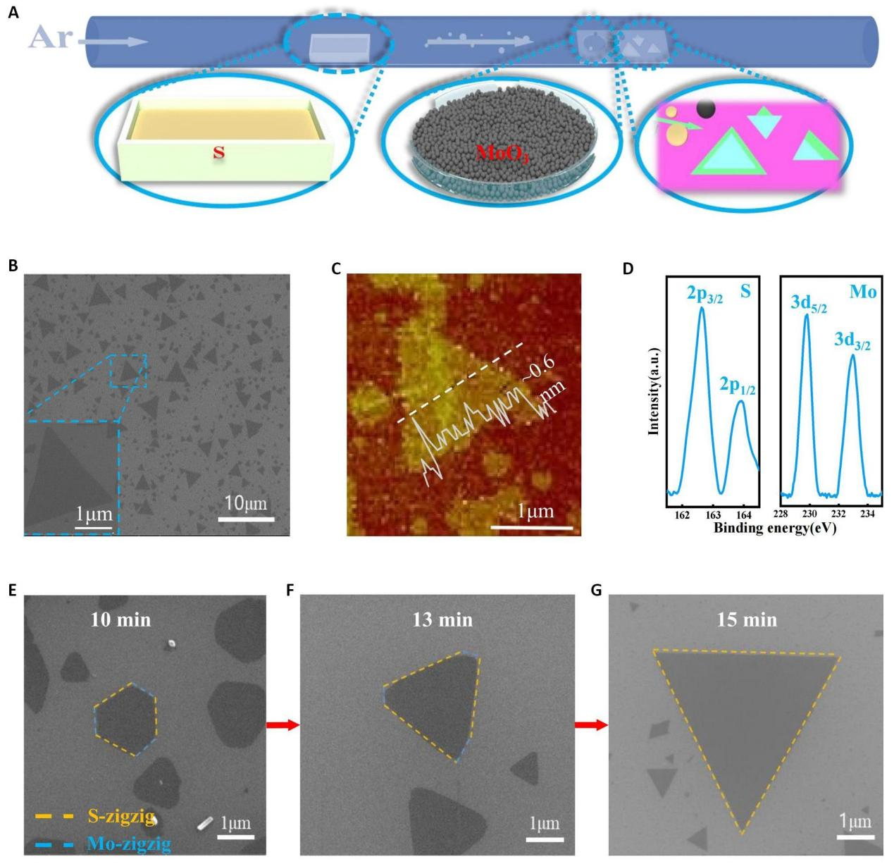
Figure 1. Controlled Growth of MoS2 Monolayers. A: Schematic diagram of MoS2 synthesis by CVD; B: SEM images of MoS2 in a triangular morphology; C: Selected region AFM images of MoS2. Inset is the corresponding height profile along the white dashed lines; D: X-ray photoelectron spectroscopy of MoS2; E-G: SEM images of MoS2 with different reaction time:10min,13min and 15min.
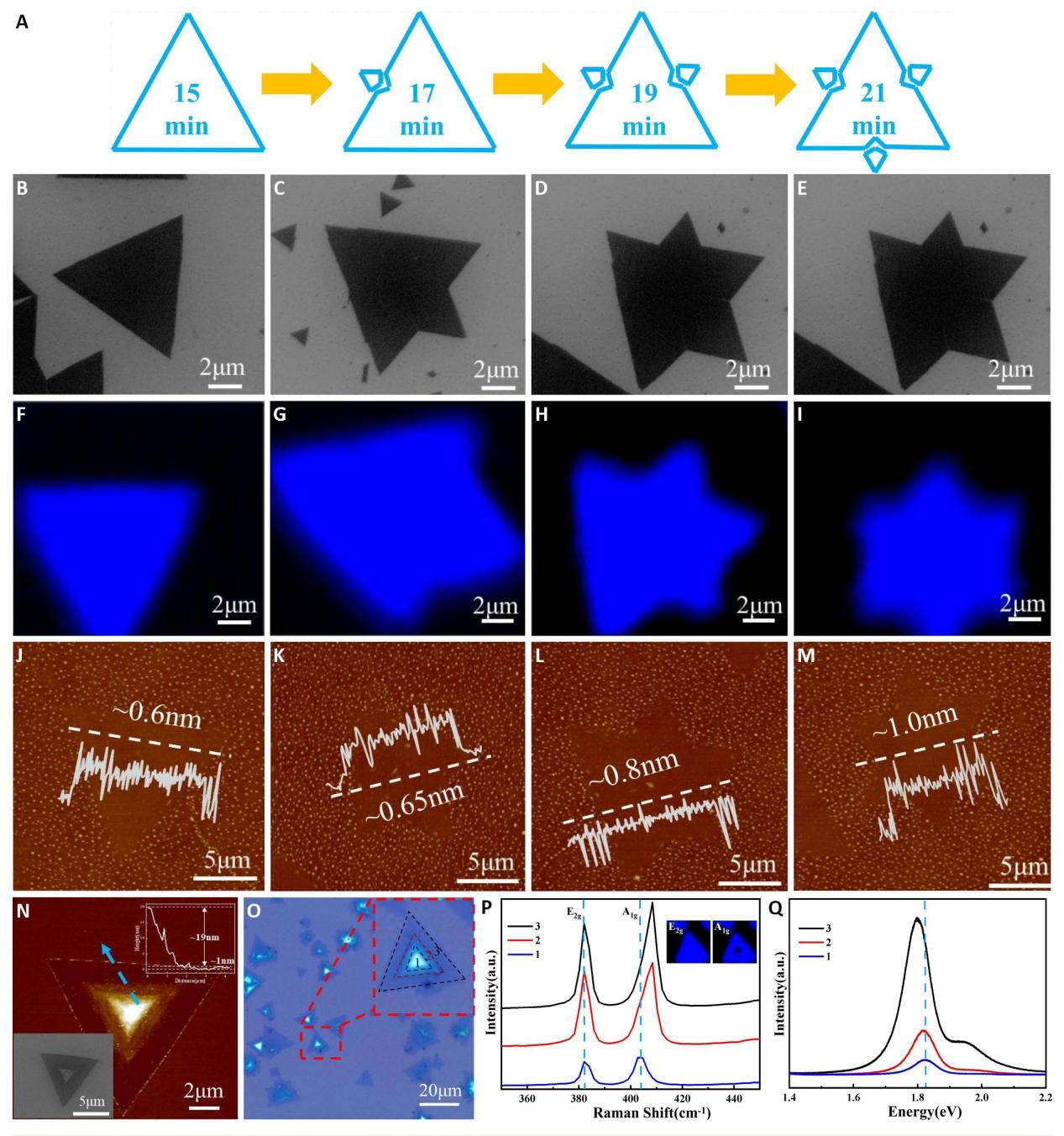
In Figure 2A-E, by further extending the growth time from 15 to 17, 19, and 21min, it can be observed that MoS2 gradually transforms from triangular to quadrangular, pentagonal, and hexagonal shapes with increasing growth time. Moreover, the longer growth periods often contain a small number of products from earlier stages, indicating the generation of new nanostructures during the evolution of the nanosheets. The uniformity of the grown materials can be partly reflected by spectral mapping. Raman spectroscopy was performed on the two different shapes of MoS2 samples, and the E2g peak positions were chosen for characterization, as shown in Figure 2F-I. It is clear that the Raman signal intensity of both triangular and polygonal-shaped single crystal MoS2 is relatively uniform, indicating the high uniformity of the MoS2 grown by chemical vapor deposition. However, due to the limitations of the testing accuracy, the small signal changes in the nucleation points and defect regions of the crystals are difficult to reflect under the conditions of spectral mapping. To accurately determine the thickness of the grown materials, AFM was performed on the differently shaped MoS2 samples, as shown in Figure 2J-M. The AFM images reveal that the surfaces of MoS2 crystals, regardless of their triangular or polygonal shapes, are highly uniform, and the height difference between the measured MoS2 crystals and the substrate is less than 1 nm. Therefore, the grown materials can be regarded as single-layer structures, and the growth occurs laterally. According to the crystal growth theory[57], the shape of crystal is determined by the growth rate of different crystal surfaces. The growth rate of Mo-zz is faster than that of S-zz, resulting in the transformation of MoS2 from hexagonal domains to triangular shapes. However, as the growth time is extended, the difference in growth rates results in the instability of boundary expansion, even causing inward concavity. The intermediate active zone with slower growth rate is easy to nucleate and grow into triangular crystal in the same way. As the growth rate of the new triangular crystal is faster, it will compress and form a grain boundary with the original crystal, ultimately resulting in a hexagonal structure of the crystal as a whole. In addition to the conventional morphology changes resulting from the growth of MoS2 crystals, their proximity during nucleation can cause them to come into contact with each other. SEM image and AFM image are shown in Figure S3A and B. Both images reveal that the two crystals merged during growth, resulting in a uniform monolayer structure with a thickness of less than 1nm. During the CVD process, the growth of monolayer MoS2 can be well-controlled by manipulating the temperature, time, gas flow rate, quality of precursor materials, and distance between the substrate and the precursor. However, some peculiar structures tend to appear in regions close to the substrate and molybdenum source, as illustrated in Figure 2N. It is noteworthy that the thickness of MoS2 in some triangular and polygonal structures is non-uniform, with decreasing thickness towards the periphery of these structures. The triangular structure had a lower thickness, approximately one monolayer, whereas the thickness increased gradually from the edge towards the center of the nanosheet, reaching a maximum at the center. This is due to the formation of Mo nuclei on the SiO2 substrate before sulfurization, where the nuclei that formed closer to the Mo source tended to be larger in size. During sulfurization, triangular MoS2 nanosheets were formed due to the differential growth rate at the edges, and unreacted Mo oxide tended to accumulate in the central region. As more sulfur was evaporated, the Mo oxide in the central region continued to react with the incoming sulfur to form triangular structures with a slightly lower growth rate, resulting in smaller triangular shapes in the center compared to the edges. Finally, a planar triangular structure with a higher thickness at the edges and a lower thickness at the center was formed.
Raman spectroscopy is a powerful tool for assessing the crystallinity of MoS2, which exhibits two prominent Raman modes, E12g and A1g. The E12g mode is known to be sensitive to long-range interlayer coupling, and the dielectric tensor is expected to increase with the number of layers. Conversely, the A1g mode is less sensitive to interlayer interactions, and is highly sensitive to surface adsorbates and electronic doping[60]. The A1g mode exhibits a strong electron-phonon coupling, which manifests itself as a red-shift and broadening of the peak with increasing doping level. Thus, the differences in the Raman mode frequencies and shifts can be utilized to determine the number of layers in MoS2. We performed Raman spectroscopy at three different positions (1, 2, and 3) on a circular MoS2 flake, as shown in Figure 2O, to investigate the layer thickness. As shown in the figure, the E12g mode undergoes a red-shift and the A1g mode undergoes a blue-shift with increasing layer thickness. The changes in the A1g mode are more pronounced than those in the E12g mode. We further performed Raman mapping at the E2g (384cm-1) and A1g (403cm-1) positions, as shown in Figure 2P. The uniform color and small peak shift of the E12g mode indicate a homogeneous growth of the MoS2 flakes. However, the non-uniform color and large peak shifts of the A1g mode suggest a significant variation in the thickness of the MoS2 flakes. It is apparent that the A1g mode is more sensitive to changes in the thickness of MoS2 flakes than the E2g mode. In addition, photoemission spectroscopy (PL) is used to analyze the above locations, as shown in Figure 2Q. It can be found that with the decrease of thickness, PL peak of MoS2 has a blue shift, which is due to the decrease of thickness. Due to the small size effect of nanomaterials, its band gap will increase in accordance with the rule of 1/d2[61]. When the nucleation points are located close to each other, contact between MoS2 nanosheets can occur. SEM and AFM were utilized to characterize this contact, as shown in Figure S4A and B, and it was found that the thickness of the nanosheet at the contact location was higher than that at the edge. Unlike the lateral growth contact of MoS2 nanosheets discussed earlier, the nanosheets in this case contact each other and terminate to form grain boundaries. Although chemical bonds have formed and terminated at the grain boundaries, diffusion of the precursor molybdenum source, which is more plentiful closer to the molybdenum source, remains active in the region where the defects are more active, resulting in excessive growth of the grain boundary surface and formation of a second-layer structure.
|
3.2 Preparation and Characterization of GaSe and Comparative Study of Photoelectric Properties between GaSe and MoS2
After preparing MoS2, it is necessary to obtain few-layer GaSe to prepare the GaSe/MoS2 heterostructure. The mechanical exfoliation method was used to prepare few-layer GaSe. Due to the strong covalent bonding within the bulk GaSe layers and weak vdW forces between the layers, GaSe is easy to separate between layers under external force and transform from bulk to few-layer structure. Figure 3A shows the optical microscopy image and AFM image of GaSe. It can be observed that the colors vary slightly on the same small piece of material, which is due to the uneven thickness of the material obtained by mechanical exfoliation. The thinner the material, the better the transparency, and the color will be closer to the substrate. The thickness of GaSe was measured by AFM as shown in Figure 3B. It was found that the thickness of GaSe material ranged from thin to thick, with values of 12nm, 21nm, 37nm, and 70nm. PL spectroscopy was used to analyze the above materials, as shown in Figure 3C. It was found that the PL peak of GaSe exhibited a blue shift, with a shift of about 4meV to higher energy, due to the decrease in thickness. Similarly, Raman spectroscopy analysis, as shown in Figure 3D, revealed that it was a β-type crystal. The excitation peaks A1g, E2g, and E1g were observed in GaSe with different thicknesses. Two A1g peaks were observed at wave numbers of 134cm-1 and 308cm-1. One of the two E2g peaks was located near 213cm-1, and the other E2g peak was theoretically expected to appear at 19cm-1, but due to the limitations of the Raman testing system, this low-frequency peak could not be observed. The intensities of the two E1g Raman peaks were the weakest among all the Raman peaks. One E1g peak appeared at 59cm-1, and the other appeared at 249cm-1, but the peaks were weak and difficult to discern in the Raman spectrum. Combining the Raman spectrum with the thickness of the material, it was found that with the increase in GaSe thickness, the A11g peak exhibited a blue shift, while the A21g peak exhibited a red shift. In addition, the E11g peak and E12g peak became more pronounced. The number of GaSe layers could be determined to be 4 based on the changes in the peak positions of the Raman spectrum.
Additionally, before fabricating the heterojunction, we fabricated individual two-dimensional devices of MoS2 (Figure 3E) and few-layer GaSe (Figure 3G), and compared their electrical properties. Under no illumination, the MoS2 device exhibited field-effect transistor behavior under gate voltage modulation, as shown in the transfer curve in Figure 3F, obtained under a source-drain bias of 1V. The transistor was in the on-state under positive gate bias, with a threshold voltage Vth of approximately -5V, indicating the N-type transport properties of the monolayer MoS2, where electrons are the majority carrier, as expected. Moreover, under a large negative gate voltage (≤ -40V), a slight hole current was observed, due to the channel inversion under the large negative voltage. The band structure of the monolayer MoS2 was induced to bend by the gate voltage, with few densities of states. The Schottky barrier formed between the metal electrode and MoS2 had a smaller effect on electrons and a larger effect on holes, leading to a large electron current and a small hole current. In contrast to the MoS2 device, as shown in Figure 3H, the output current of the GaSe device decreased with increasing gate voltage, and the device was in the on-state under negative gate bias, with holes as the majority carrier, indicating the typical P-type transport properties of GaSe, laying the foundation for the subsequent construction of the GaSe/MoS2 P-N junction. For a field-effect transistor, the conductance (gm), electron mobility (μ), on/off current ratio, and threshold voltage swing (SS) are all important metrics for assessing its electrical transport performance. The conductance primarily describes the strength of current transmission ability of the field-effect transistor under the regulation of forward gate voltage for opening. The formula for its calculation is as follows:
$$ {g}_{m}=\frac{{dI}_{ds}}{{dV}_{g}}\left(3\right)$$
Where Ids is the source-drain current and Vg is the gate voltage. Based on the linear portion of the transfer curve, we determined the conductance of a single-layer MoS2 FET to be 1.32nS. The electron mobility describes the directed drift velocity of electrons under the influence of an external electric field. Combined with the previously obtained gm, it can be calculated using the following formula:
$$ {\mu }=\left[\frac{L}{W{C}_{i}{V}_{ds}}\right]\times {g}_{m}\left(4\right)$$
$$ {C}_{i}=\frac{{\epsilon }_{0}{\epsilon }_{r}}{d}\left(5\right)$$
Where μ is the electron mobility, L and W denote the length and width of the device channel material, respectively, and Ci represents the capacitance of the dielectric layer. The vacuum permittivity ε0 is 8.854×10⁻¹²F·m-1, while the dielectric constant of silicon dioxide, εr, is 3.9. The thickness of the silicon dioxide dielectric layer, d is 300nm. Consequently, the calculated electron mobility value for a single-layer MoS2 FET is 0.008cm2V-1s-1. The current on-off ratio is defined as the ratio of the maximum current in the on-state to the minimum current in the off-state under the modulation of gate voltage. The on-off ratio of the monolayer MoS2 field-effect transistor can be calculated from the exponential transfer curve shown in Figure 3F, which is 4.34×10⁵. To meet the practical requirements of high-performance integrated digital logic circuits, an on-off ratio greater than 104 is a basic requirement, and the on-off ratio of the monolayer MoS2 field-effect transistor obviously satisfies this requirement. In addition, the threshold voltage swing (SS) is defined as the voltage required for the current to increase by one order of magnitude. It can be calculated using the data from the maximum slope of the exponential part of the transfer curve as follows:
$$ {S}{S}=\frac{{dV}_{g}}{d{{log}I}_{ds}}\left(6\right)$$
where SS is the threshold voltage swing, Vg is the gate voltage, and Ids is the source-drain current. By calculating the data of the maximum slope of the exponential transfer curve (-20V~ -10V), we obtain a threshold voltage swing value of 9V/s for a monolayer MoS2 field-effect transistor with a silicon dioxide dielectric layer. Although the MoS2 field-effect transistor can be effectively controlled over a range of gate voltages from -60V to 60V, with a large on-off ratio of 4.34×10⁵ and a wide control range, its carrier mobility is relatively small and its threshold swing is relatively large. It is clear that the device's electrical transport performance is average and is not particularly sensitive to changes in gate voltage, making it unable to respond as quickly as possible under gate voltage control. Similarly, according to formulas (2) and (4), the carrier mobility and threshold swing of the GaSe device can be calculated. It can be found that although the on-off ratio of the GaSe device is only about 103, its carrier mobility μ is 0.08cm2V-1s-1 and the threshold swing SS is approximately 3V/s. Compared to MoS2, GaSe has more excellent carrier transport performance.
|
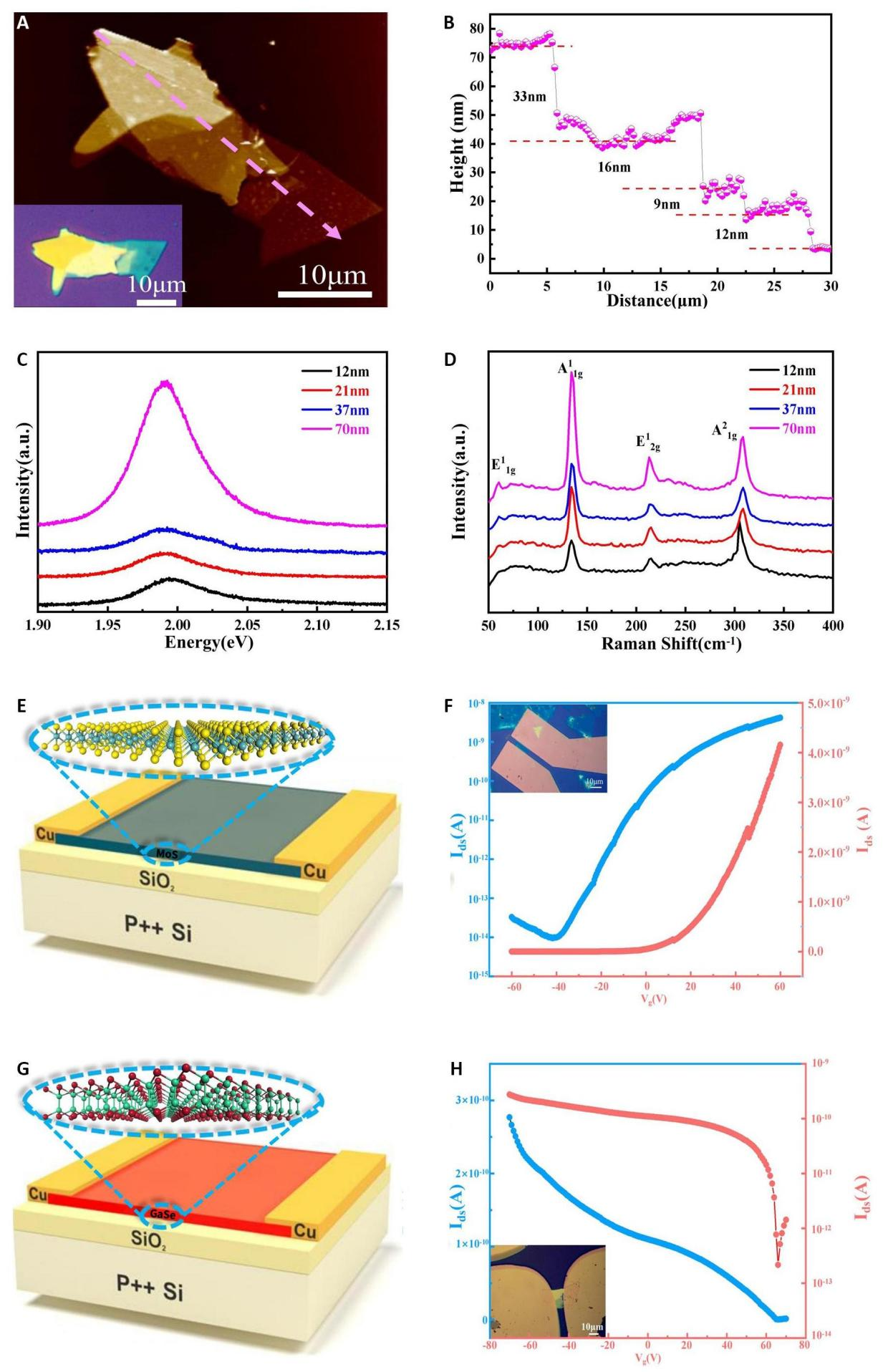
Figure 3. Characterization of Few-layer GaSe and Two-Dimensional Devices. A: Selected region AFM images of few-layer GaSe. Inset is the optical image of GaSe; B: Corresponding height profile along the dashed lines of GaSe; C: PL spectra of few-layer GaSe in different height; D: Raman spectra of longitudinally stacked GaSe in different height; E: Schematic diagram of two-dimensional MoS2 device; F: Transfer curve of two-dimensional MoS2 device. Inset is the optical image of the MoS2 device; G: Schematic diagram of two-dimensional GaSe device; H: Transfer curve of two-dimensional GaSe device. Inset is the optical image of the GaSe device.
3.3 Study on the Photoelectric Heterojunction Performance of GaSe/MoS2
The MoS2/GaSe vertical heterojunction was constructed by transferring MoS2 and GaSe using a transfer platform, and the schematic diagram of the heterojunction is shown in Figure 4A. Then UV-Vis absorption spectroscopy was carried out and compared with the results of the MoS2 film, as shown in Figure 4B. The figure shows that the optical absorption of MoS2 with covered GaSe is slightly enhanced compared to the MoS2 film, and the enhancement is more significant in the ultraviolet region. To test the response of the photodetectors to monochromatic light of different wavelengths, monochromatic light of different wavelengths obtained by passing through a spectrometer with a xenon lamp as the light source was vertically irradiated on the surface of the photodetectors. According to the above results of ultraviolet absorption, the wavelengths of the monochromatic excitation light used were 300nm, 350nm, 400nm, 450nm, 500nm, 550nm, 600nm, 650nm, and 700nm, respectively. By controlling the light source current, slit width, and aperture size, the power density of each monochromatic light obtained by the spectrometer can be ensured to be basically the same, which is 0.528mW/cm2. Figure 4C and Figure 4D show the light response curves of the single-layer MoS2 photodetector under excitation by light of different wavelengths. Under the condition of no light illumination, the current only reached about 0.1nA after applying a voltage of 5V to the single-layer MoS2 photodetector. Under the excitation of 700nm wavelength, the current change was not obvious relative to other wavelength conditions, which also corresponds to the above ultraviolet absorption results. With the decrease of the wavelength, the current under 5V applied voltage gradually increased from 0.1nA to nearly 50nA, indicating that it has a wide range of light response intervals, i.e., from ultraviolet light (300nm) to visible light (650nm) with strong response. In addition, in order to investigate which smaller wavelength range in the ultraviolet region is more sensitive for the single-layer MoS2 photodetector, the wavelength range was adjusted to 300-400nm using a spectrometer, and tests were conducted every 10nm of wavelength, while still controlling the light power density at around 0.528mW/cm2 by adjusting the aperture, slit, and power supply current. The light response results are shown in Figure S5A-B. Observations reveal that the ratio of illumination current to dark current under 5V reached only 47 when the response was weakest (400nm), while it was as high as 367 when the response was strongest (330nm). Therefore, even though the single-layer MoS2 photodetector has a strong response in the 300-400nm ultraviolet region, there is a significant difference in different small segments within it, and such a fine differentiation is a very important characteristic for exploring a photodetector specific to a certain wavelength. In Figure 4E-F, by analyzing the output curves, we observe that the current-voltage relationship in the devices fabricated on the GaSe/MoS2 heterojunction remains linear under low voltage, indicating a non-rectifying Ohmic contact between the electrode and the material. Notably, the current increases with a higher rate under 300-350nm excitation than other wavelengths, and eventually reaches saturation. Under a voltage of 5V, the output current for the 300-400nm range is more than 10 times greater than for the 400-700nm range, as observed in the single-layer MoS2 photodetector. However, the GaSe/MoS2 photodetector exhibits an overall higher output current than MoS2. For single-layer MoS2 photodetectors, the photocurrent is intricately influenced by various factors, including the excitation wavelength, source-drain voltage, and the power density of the incident light. Figure 4G elucidates the intricate relationship by presenting the output curves of a single-layer MoS2 photodetector under different power densities of 350nm excitation light. A comprehensive analysis of these curves in comparison to the dark state output curve reveals a discernible trend: as the light power density escalates, the photocurrent exhibits a steeper slope with respect to the source-drain voltage. In Figure 4H, as the light intensity increases, the photocurrent exhibits a linear growth, in contrast to the MoS2 photodetector, which approaches a saturation state at higher light powers. This disparity can be attributed to the excitation of a larger number of charge carriers under higher light power conditions. Consequently, the inhibitory effect of the GaSe/MoS2 heterojunction on electron-hole recombination is magnified, leading to a substantial amplification of the photocurrent.
To better compare the response of the monolayer MoS2 photodetector under monochromatic light of different wavelengths, we used the photocurrent at a source-drain voltage of 1V as the criterion. The photocurrent is defined as the difference between the photocurrent and the dark current, that is:
$$ {I}_{pℎ}={I}_{illumination}-{I}_{dark}\left(7\right)$$
Figure 4I shows the photocurrent of the photodetectors under different monochromatic light irradiation at 1V. It can be seen that the photocurrents at a wavelength of 300-400nm is significantly higher than that at a wavelength of 400-650nm, by an order of magnitude, and the illumination current at a wavelength of 350nm is also significantly higher than that at 300nm and 400nm. Therefore, the photodetectors have the largest response in the ultraviolet region, mainly detecting light with a wavelength of 300-400nm. However, in the previous ultraviolet absorption test, the position of the highest light absorption intensity was in the range of 400-450nm, which deviates from the corresponding result here. Thus, light absorption of the material can only be a prerequisite for light response, but the result of light absorption cannot fully reflect the change in light response. Generally, the light response value (R) and the detectivity (D*) are important indicators for evaluating the photodetection performance of the photodetectors. The light response value (R) can be defined as the photocurrent generated per unit power and per unit area, calculated by the following formula:
$$ {R}=\frac{{I}_{pℎ}}{PS}\left(8\right)$$
In the above equation, R represents the photoresponsivity, Iph is the photocurrent, P is the power of the incident light, and S is the effective area of the photoactive channel in the detector. The performance of a photoactive material is generally influenced by three types of noise: dark current noise, Johnson noise, and thermal noise. Among them, dark current noise usually has the greatest impact, so the detectivity (D*) is typically calculated using the following equation:
$$ {D}^{\ast }=\frac{R{A}^{\frac{1}{2}}}{{\left(2e{I}_{d}\right)}^{\frac{1}{2}}}\left(9\right)$$
Where D* represents the detectivity, R represents the responsivity, A represents the effective photoactive area of the phototransistor, e represents the elementary charge, and Id represents the dark current. According to Equations (9) and (10), the responsivity and detectivity of photodetectors in the wavelength range of 300-700nm at a source-drain voltage of 1V were calculated and the results are shown in Figure 4J-K. It can be observed that the GaSe/MoS2 photodetector exhibited enhanced performance in terms of photocurrent, responsivity, and detectivity compared to the single-layer MoS2 photodetector, with a more significant improvement in the wavelength range of 300-400nm. Specifically, under excitation at 300nm, the GaSe/MoS2 photodetector achieved a responsivity of 42.6A/W and a detectivity of 8.17×10¹²Jones, which is three times that of the MoS2 photodetector. The improved optoelectronic performance can be attributed to the band structure coupling of MoS2 and GaSe, which can promote the separation of electrons and holes and prevent their recombination, leading to an increase in the number of carriers and an effective increase in the photocurrent. Additionally, the absorption characteristics of GaSe in the ultraviolet wavelength range enhances the response of the GaSe/MoS2 photodetector in the range of 300-400nm. To elucidate the intricate interplay between photocurrent and light power density, we extracted the photocurrent data corresponding to a source-drain voltage of 1V under varying light power densities (Figure 4I). Remarkably, the data unequivocally demonstrates a linear increase in photocurrent with low light power densities (below 0.564mW/cm2). However, as the light power density surpasses this threshold, the photocurrent growth tapers, ultimately reaching a saturation state. Further investigation involved calculating the response value (R) and detectivity (D*) at different light power densities, as shown in Figure 4M-N. Both the response value (R) and detectivity (D*) display a diminishing trend as the light power density escalates, indicative of defect scattering between the single-layer MoS2 and the dielectric layer. At the same time, we observed consistent trends in the variations of the light response value and detectivity in both photodetector configurations, with a gradual decrease as the light power density escalates. Notably, the GaSe/MoS2 photodetector outperforms its counterpart, exhibiting superior optoelectronic properties. Notably, at a light power density of 0.008mW/cm2, the GaSe/MoS2 photodetector attains an impressive light response value of 52.2A/W and detectivity of 1×10¹³Jones.
Furthermore, it is imperative to subject the device to long-term performance testing, as the presented results are based on short-term light illumination and applied voltage conditions. The response speed assumes paramount importance as a key indicator of photodetection device quality. It is defined as the time required for the current to reach 80% of its maximum value upon activating or deactivating the excitation light. To evaluate the response speed and stability of the single-layer MoS2 photodetector, we conducted thorough testing under various conditions. Figure S6A-C present the I-t curves for 350nm, 450nm, and 550nm wavelength illuminations, with an applied voltage of 1V. Each cycle consisted of a controlled light illumination and dark period, both lasting 300sec. Comparing the previous findings on light response, a clear pattern emerges as the wavelength decreases. Remarkably, under nearly identical dark current conditions, the single-layer MoS2 photodetector exhibits a substantial enhancement in photocurrent upon light excitation, accompanied by a noticeable reduction in current during the dark period. This observation suggests that the recombination of charge carriers is facilitated more efficiently in the higher current state. Consequently, relative to other wavelengths, the single-layer MoS2 photodetector displays heightened sensitivity in the ultraviolet range, particularly at shorter wavelengths. However, it is important to note that although the light-dark cycling ensures waveform stability and reproducibility, the 300sec light exposure is insufficient to achieve current saturation, and the subsequent 300sec dark period does not reduce the current to the initial dark current level. Thus, the response time of the device extends to the order of hundreds of milliseconds, indicating a relatively slow response speed. This characteristic can be attributed to inherent defects within the material arising from the chemical vapor deposition growth technique. These defects impede the immediate and efficient excitation of most charge carriers upon light activation. Furthermore, during the light-off state, certain defects act as “traps” that impede the recombination of electrons and holes, necessitating a sufficiently long time for the current to return to its baseline level. Additionally, the testing was conducted under ambient conditions where the MoS2 surface readily adsorbs oxygen and water vapor, leading to charge trapping and consequently compromising the optoelectronic properties. Despite the relatively slow response speed of the single-layer MoS2 photodetector, hindering instantaneous light-on and light-off transitions, visual analysis reveals excellent repeatability and stability of the device. To evaluate the long-term response at different wavelengths, an alternative metric, the light-to-dark response ratio, proves insightful. This ratio quantifies the stable light-induced current relative to the dark current during the light-dark cycle. Notably, the light-to-dark response ratio for the single-layer MoS2 photodetector at excitation wavelengths of 450nm and 550nm remains below 2, while at 350nm, it reaches approximately 3. These findings corroborate the rapid response exhibited by the single-layer MoS2 photodetector at 350nm. In Figure S7A-D, To investigate the response speed and stability of the single-layer MoS2 photodetector at different light power densities, we conducted a comprehensive analysis using 350nm monochromatic light with fixed 300sec durations for both the light-on and light-off states. Consistent with previous observations, we found that the 300sec duration was insufficient to reach current saturation during the light-on state or restore the current to its baseline level during the light-off state, indicating a relatively slow response speed. However, a closer examination of the obtained curves revealed intriguing insights into the device's behavior. Particularly, at lower light power densities, specifically at 0.008mW/cm2, we observed a smaller increase in current during the 300sec light-on period, even diminishing by an order of magnitude. This finding suggests that the single-layer MoS2 photodetector exhibits enhanced detection performance only when the incident light intensity exceeds a certain threshold. This phenomenon can be attributed to the complex interplay between charge carrier generation, recombination, and trapping dynamics, which become more prominent at higher light power densities. Furthermore, the reduced number of electrons transitioning to the conduction band at lower power densities was counteracted by the slower electron-hole recombination, resulting in a gradual convergence towards a stable state with a smaller decrease in current during the light-off state. This behavior elucidates the observed increase in peak current over time and highlights the intricate charge carrier dynamics involved in the device's operation. Additionally, a comparative analysis of the I-t curves across the four different light power densities revealed a progressive enhancement in the light-to-dark response ratio with increasing power densities. Notably, at an illumination intensity of 1.215mW/cm2, the light-to-dark response ratio reached an impressive value of 3.34. These findings underscore the significant role of higher light power densities in improving the photodetection performance of the single-layer MoS2 photodetector, particularly in terms of its light-induced response relative to its dark current characteristics.
Based on the conclusive data obtained from the preceding experimental analysis, it is unequivocally evident that the GaSe/MoS2 photodetector exhibits a robust and discernible response within the ultraviolet spectral region. Consequently, we delved into an in-depth investigation of the photodetector’s stability under varying light intensities at a precise excitation wavelength of 350nm. The I-t characteristics of both the GaSe/MoS2 and MoS2 photodetectors under two meticulously selected light intensities, namely 0.564mW/cm2 and 1.215mW/cm2, are meticulously portrayed in Figure 4O-P. The GaSe/MoS2 photodetector demonstrates comparable response time to the MoS2 photodetector. Despite the fact that the 300sec light exposure does not rapidly elevate the device’s dark current to a saturated state, an improvement in response speed is observed. Particularly noteworthy is the enhanced performance in terms of light-to-dark current ratio. Within the same 300sec duration, the photodetector effectively raises the low dark current to a higher level under illumination and reduces the elevated current back to its original dark current level. Notably, at a light power density of 0.564mW/cm2, the light-to-dark current ratio increases from 3 to 5.57, while at a power density of 1.215mW/cm2, it increases from 3.38 to 5.75.
|
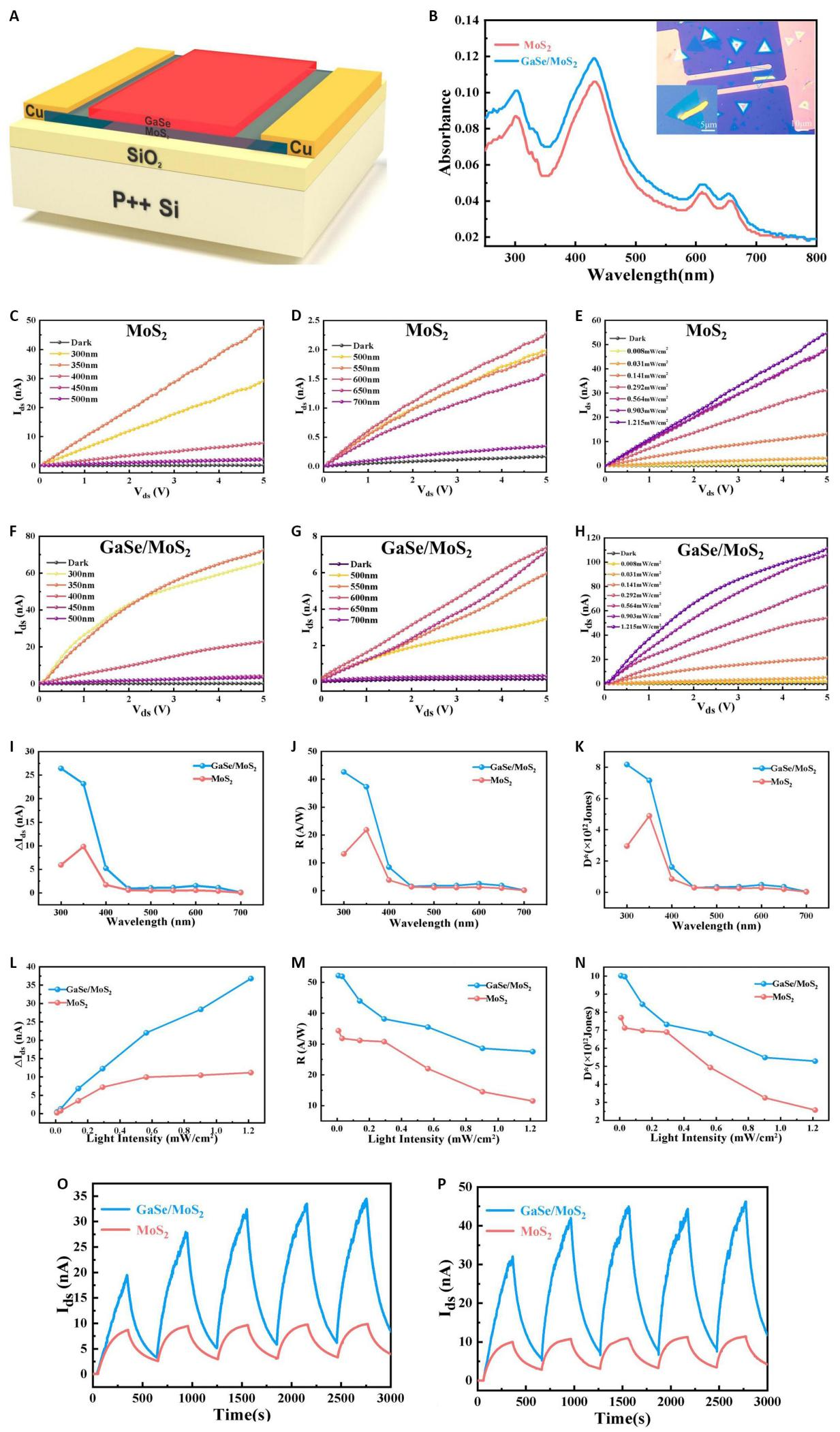
Figure 4. Fabrication and Properties of GaSe/MoS2 Photodetectors. A: Schematic diagram of GaSe/MoS2 photodetector; B: UV-Vis absorption spectroscopy of GaSe/MoS2 heterojunction and monolayer MoS2. Insets are the optical images of the GaSe/MoS2 photodetector; C-D: Output curves of MoS2 photodetector under 300-700nm monochromatic light with intensity of 0.564 mW/cm2; E-F: Output curves of GaSe/MoS2 photodetector under 300-700nm monochromatic light with intensity of 0.564mW/cm2; G-H: Output curves of MoS2 and GaSe/MoS2 photodetectors under different light intensities at 350nm wavelength; I-K: Performance of MoS2 and GaSe/MoS2 photodetectors under 300-700nm monochromatic light with intensity of 0.564mW/cm2; (I) photocurrent; (J) photoresponsivity; (K) detectivity; L-N: Performance of MoS2 and GaSe/MoS2 photodetectors under different light intensities at 350nm wavelength:(L) photocurrent; (M) photoresponsivity; (N) detectivity; O-P: I-t curves of MoS2 and GaSe/MoS2 photodetectors under different light intensities at 350nm wavelength:(O) 0.564mW/cm2; (P) 1.215mW/cm2.
Based on the previous electrical performance tests, it is evident that the MoS2 synthesized by chemical vapor deposition is an n-type material, whereas the mechanically exfoliated GaSe is a p-type material. Consequently, the photovoltaic device formed by these two materials also functions as a vertical P-N junction as shown in Figure 5A-B. To evaluate the photovoltaic performance of the GaSe/MoS2 device, we conducted photodetection experiments under varying wavelengths (300nm, 350nm, 400nm, 450nm, and 500nm) of incident light at a density of 0.564mW/cm2. Figure 5C presents the output characteristics of the device under dark and different light wavelengths. The rectification effect, indicating directional conductivity, is evident in the GaSe/MoS2 heterojunction device, resembling the electrical characteristics of a photodiode. Additionally, a photovoltaic effect is observed in this device when the output voltage and current are both zero, as shown in the inset in Figure 5C. This phenomenon is absent in traditional two-dimensional material-based photodetectors. The P-N junction serves not only as a fundamental unit in diodes and photodetectors but also as a crucial component in solar cells. Therefore, the subsequent investigation will primarily focus on the photovoltaic effect of the GaSe/MoS2 vertical heterojunction. Under dark conditions, the device exhibits minimal current when the output voltage is 0. However, when illuminated with ultraviolet light in the range of 300-400nm, the device demonstrates noticeable open-circuit voltage (Voc) and short-circuit current (Isc). For wavelengths between 300nm and 400nm, the Voc values are measured as 0.124mV, 0.131mV, and 0.118mV, while the Isc values are -0.003nA, -0.007nA, and -0.001nA, respectively. Photovoltaic devices offer a promising avenue for the conversion of solar energy into electrical power. The quantification of converted power (Pel) can be accomplished using the equation:
$$ {P}_{el}={I}_{ds}\times {I}_{ds}\left(10\right)$$
Where Pel represents the electrical power, Ids denotes the source-drain current, and Ids signifies the source-drain voltage. By analyzing the curve presented in Figure 5C, the device's output current under varying applied voltages can be determined. Subsequently, employing the aforementioned equation enables precise calculation of the electrical power, facilitating a rigorous evaluation of the GaSe/MoS2 vertical heterojunction device’s solar energy conversion efficiency. The Figure 5D illustrates the computed power curves for different excitation light intensities. Remarkably, at the wavelength of 300nm, the maximum electrical power reaches 9.361×10⁻⁵pW, while at 400nm, it amounts to 3.163×10⁻⁵pW. Notably, the peak electrical power is achieved at the wavelength of 350nm, with a value of 2.157×10⁻⁴pW. Upon acquiring measurements for short-circuit current, open-circuit voltage, and electrical power, fill factor (FF) can be calculated. The fill factor represents the ratio of the electrical power (Pel,m) to the product of the short-circuit current (Isc) and open-circuit voltage (Voc). It can be expressed using the following equation:
$$ {F}{F}=\frac{{P}_{el,m}}{\left({I}_{sc}{V}_{oc}\right)}\left(11\right)$$
Employing this equation, the fill factors at different wavelengths, namely 300nm, 350nm, and 400nm, are determined as 0.25, 0.24, and 0.27, respectively. These results suggest that the fill factor of the GaSe/MoS2 vertical heterojunction device exhibits negligible dependence on the wavelength within the ultraviolet range. Another vital performance indicator for characterizing the photovoltaic capability is the energy conversion efficiency (ηpv), which quantifies the device’s ability to convert incident light energy into electrical energy. The energy conversion efficiency can be calculated using the following formula:
$$ {\eta }_{PV}=\frac{{P}_{el,m}}{{P}_{OPT}}\left(12\right)$$
Herein, ηpv represents the energy conversion efficiency, Pel,m denotes the maximum electrical power, and POPT signifies the applied optical power. Given the fixed optical power density of 0.564mW/cm2, the energy conversion efficiency of the GaSe/MoS2 vertical heterojunction device can be evaluated by considering the illuminated area. However, even at the wavelength of 350nm, where the output electrical power is maximized, the energy conversion efficiency remains at a modest 0.00028%. This indicates that there is considerable room for improvement in the performance of this heterojunction device. To further explore performance variations, particularly regarding the relatively high energy conversion efficiency observed at the 350nm wavelength, the device was subjected to changes in light intensity. Figure 5E illustrates the output characteristics of the GaSe/MoS2 vertical heterojunction device at light intensities of 0.292mW/cm2, 0.564mW/cm2, 0.903mW/cm2, and 1.215mW/cm2. It becomes apparent that as the light power density increases, both the open-circuit voltage (Voc) and short-circuit current (Isc) demonstrate an upward trend. Additionally, the electrical power under different applied voltages was computed, as shown in Figure 5F. The maximum output electrical power rises with increasing light intensity, reaching values of 1.158×10⁻⁴pW, 2.157×10⁻⁴pW, 2.837×10⁻⁴pW, and 5.421×10⁻⁴pW, respectively. The fill factor consistently hovers around 0.25 for different light intensities, suggesting no significant correlation. However, concerning energy conversion efficiency, the values remain approximately 0.00028% for lower light powers. Interestingly, when the light power density reaches 1.215mW/cm2, the energy conversion efficiency experiences a modest improvement, reaching 0.00033%, an increase of approximately 18%. These results indicate that a discernible trend emerges when the light power density reaches a certain threshold.
|
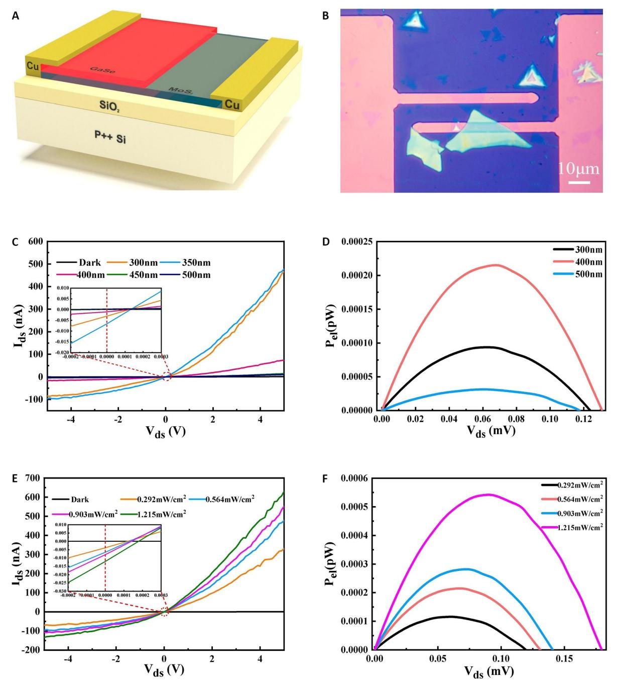
Figure 5. Fabrication and Properties of GaSe/MoS2 Photovoltaic Device. A: Schematic diagram of GaSe/MoS2 photovoltaic device; B: Optical image of the GaSe/MoS2 photovoltaic device; C: Output curve of GaSe/MoS2 photovoltaic device under 300-500nm monochromatic light with intensity of 0.564mW/cm2; D: The curve of electric power as a function of source-drain voltage under 300-500nm monochromatic light with intensity of 0.564mW/cm2; E: Output curves of GaSe/MoS2 photovoltaic device under different light intensities at 350nm wavelength; F: The curve of electric power as a function of source-drain voltage under different light intensities at 350nm wavelength.
|
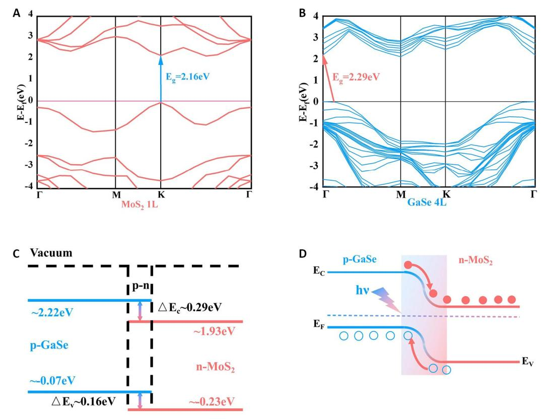
Figure 6. Electronic Band Structures and Photocurrent Mechanism of the GaSe/MoS2 Heterostructure. A: Energy band diagram for monolayer MoS2; B: Energy band diagram for few-layer GaSe; C: Band-edge positions of few-layer GaSe and monolayer MoS2 relative to the vacuum level; D: Energy band diagram of the GaSe/MoS2 heterojunction.
Furthermore, understanding the electronic properties and charge dynamics in heterostructures is crucial for the development of next-generation optoelectronic devices. We investigated the band alignment and photocurrent generation in GaSe/MoS2 heterostructures. As evidenced by the calculation results, it is evident that monolayer MoS2 behaves as a direct bandgap semiconductor with a bandgap value of 2.16eV as shown in Figure 6A, while few-layer GaSe exhibits characteristics of an indirect bandgap semiconductor with a bandgap value of 2.29eV as shown in Figure 6B. These findings are in accordance with previous reports[55]. Figure 6C illustrates the band alignment between monolayer MoS2 and two-layer GaSe relative to the vacuum level. It is visually apparent that the GaSe/MoS2 heterostructure forms a type-II band alignment, with ΔEc of approximately 0.29eV and ΔEv of around 0.16eV. Upon closer examination of Figure 6D, it becomes clear that when MoS2 and GaSe come into contact to form a heterojunction, the disparity in the Fermi energy levels of the two materials results in a concentration gradient of the main carriers at the interface. To achieve equilibrium in the Fermi energy levels, free electrons diffuse towards the GaSe side, leading to an increase in the number of holes on the MoS2 side. Simultaneously, under external illumination conditions, the holes and electrons generated undergo recombination at the MoS2/GaSe interface. Consequently, the GaSe side, which predominantly contains holes, experiences a reduction in hole count, while the majority of the recombined electrons assume a negative charge state. Conversely, the MoS2 side, which predominantly contains electrons, loses electrons, resulting in a net positive charge at the macro level. As a result of these factors, at the junction of GaSe and MoS2, where both materials have lost their respective charge carriers, a depletion layer is formed—a region comprised solely of positive and negative ions. This depletion layer arises due to the aforementioned reasons. The aforementioned phenomena lead to the MoS2 side exhibiting a positive charge due to the loss of electrons, while the GaSe side manifests a negative charge due to the reduction in holes. This charge separation engenders an internal electric field between the two dissimilar semiconductors, with the N region of the electric field pointing towards the P region. Driven by a robust built-in electric field, electrons in the vicinity of the GaSe side drift towards the MoS2 direction, while holes near MoS2 migrate towards the GaSe direction. Subsequently, the separated electrons and holes are collected by the electrode, generating a substantial amount of photocurrent under short-circuit conditions.
4 CONCLUSIONS
In summary, we demonstrate the controllable synthesis of monolayer MoS2 through chemical vapor deposition, offering a viable approach for the fabrication of MoS2/GaSe heterojunctions. Leveraging this synthesis technique, we construct photodetectors and photovoltaic devices based on GaSe/MoS2 heterojunctions that exhibit exceptional performance. The photodetector surpasses its monolayer MoS2 counterpart, achieving a remarkable photo-responsivity of 42.6A/W and a detectivity of 8.17×10¹²Jones under 300nm excitation with a light power density of 0.564mW/cm2, representing a threefold improvement. Furthermore, the photovoltaic device demonstrates a pronounced photovoltaic effect in the ultraviolet region, with a fill factor consistently around 0.25 and an energy conversion efficiency of 0.00033% at 350nm wavelength. Our findings present an effective strategy for the controlled synthesis of heterostructures using two-dimensional materials and offer selectable insights for future advancements in optoelectronic device applications.
Acknowledgments
The authors acknowledge the financial support from the Heilongjiang Provincial Natural Science Foundation of China No. YQ2022E024 and the National Natural Science Foundation of China No. 52375327.
Conflicts of Interest
The authors declare that they have no conflict of interest.
Data Availability
The raw/processed data required to reproduce these findings cannot be shared at this time due to technical limitations.
Copyright Permissions
Copyright © 2024 The Author(s). Published by Innovation Forever Publishing Group Limited. This open-access article is licensed under a Creative Commons Attribution 4.0 International License (https://creativecommons.org/licenses/by/4.0), which permits unrestricted use, sharing, adaptation, distribution, and reproduction in any medium, provided the original work is properly cited.
Author Contribution
Li Z conducted formal analysis and contributed to the writing of the original draft, as well as participated in the review and editing process. Shao J was responsible for DFT calculations and also contributed to formal analysis. Wang Z contributed to the writing of the original draft and participated in formal analysis. Zhu P was involved in formal analysis and contributed to the writing of the original draft. Pang J contributed to formal analysis. He P handled project administration duties, while Zhang S provided supervision throughout the project.
Abbreviation List
2D, Two-dimensional
AFM, Atomic force microscopy
CVD, Chemical vapor deposition
Mo-zz, Mo zigzag,
PL, Photoluminescence
S-zz, S zigzag,
TMDCs, Two-dimensional transition metal dichalcogenides
vdW, Van der Waals
References
[1] Han J, Wang F, Han S et al. Recent Progress in 2D Inorganic/Organic Charge Transfer Heterojunction Photodetectors. Adv Funct Mater, 2022; 32: 2205150.[DOI]
[2] Tian R, Gan X, Li C et al. Chip-integrated van der Waals PN heterojunction photodetector with low dark current and high responsivity. Light-Sci Appl, 2022; 11: 101.[DOI]
[3] Huo N, Konstantatos G. Recent Progress and Future Prospects of 2D-based Photodetectors. Adv Mater, 2018; 30: 1801164.[DOI]
[4] Zha J, Luo M, Ye M et al. Infrared Photodetectors Based on 2D Materials and Nanophotonics. Adv Funct Mater, 2022; 32: 2111970.[DOI]
[5] Do D P, Hong C, Bui V Q et al. Highly Efficient van der Waals Heterojunction on Graphdiyne toward the High-performance Photodetector. Adv Sci, 2023; 10: 2300925.
[6] Xu Z, He M, Wu Q et al. Ultrafast Charge Transfer 2D MoS2/Organic Heterojunction for Sensitive Photodetector. Adv Sci, 2023; 10: 2207743.[DOI]
[7] Boudiaf K, Bouhemadou A, Boudrifa O et al. Structural, Elastic, Electronic and Optical Properties of LaOAgS-Type Silver Fluoride Chalcogenides: First-Principles Study. J Electron Mater, 2017; 46: 4539-4556.[DOI]
[8] Wu D, Tian R, Lin P et al. Wafer-scale synthesis of wide bandgap 2D GeSe2 layers for self-powered ultrasensitive UV photodetection and imaging. Nano Energy, 2022, 104: 107972.[DOI]
[9] Hu X, Li X, Li G et al. Recent Progress of Methods to Enhance Photovoltaic Effect for Self-powered Heterojunction Photodetectors and Their Applications in Inorganic Low-dimensional Structures. Adv Funct Mater, 2021, 31: 2011284.[DOI]
[10] Wang H, Gao S, Zhang F et al. Repression of Interlayer Recombination by Graphene Generates a Sensitive Nanostructured 2D vdW Heterostructure Based Photodetector. Adv Sci, 2021, 8: 2100503.[DOI]
[11] Wang T, Zheng D, Zhang J et al. High-performance and Stable Plasmonic-functionalized Formamidinium-based Quasi-2D Perovskite Photodetector for Potential Application in Optical Communication. Adv Funct Mater, 2022, 32: 2208694.[DOI]
[12] Benkabou A, Bouafia H, Sahli B et al. Structural, elastic, electronic and thermodynamic investigations of neptunium chalcogenides: First-principles calculations. Chinese J Phys, 2016; 54: 33-41.[DOI]
[13] Yu X, Wang X, Zhou F et al. 2D van der Waals Heterojunction Nanophotonic Devices: From Fabrication to Performance. Adv Funct Mater, 2021; 31: 2104260.[DOI]
[14] Lee CH, Park Y, Youn S et al. Design of p-WSe2/n-Ge Heterojunctions for High-Speed Broadband Photodetectors. Adv Funct Mater, 2022; 32: 2107992.[DOI]
[15] Konstantatos G. Current status and technological prospect of photodetectors based on two-dimensional materials. Nat Commun, 2018; 9: 5266.[DOI]
[16] Al-Douri Y, Khachai H, Khenata R. Chalcogenides-based quantum dots: Optical investigation using first-principles calculations. Mat Sci Semicon Proc, 2015; 39: 276-282.[DOI]
[17] Fu Q, Wang X, Liu F et al. Ultrathin Ruddlesden–popper Perovskite Heterojunction for Sensitive Photodetection. Small, 2019; 15: 1902890.[DOI]
[18] Aftab S, Hegazy HH.. Emerging Trends in 2D TMDs Photodetectors and Piezo-phototronic Devices. Small, 2023; 19: 2205778.[DOI]
[19] An J, Zhao X, Zhang Y et al. Perspectives of 2D Materials for Optoelectronic Integration. Adv Funct Mater, 2022; 32: 2110119.[DOI]
[20] Al-Douri Y, Hashim U. Chalcogenide nanostructures: Topography, synthesis, properties, and applications. J Renew Sustain Ener, 2014; 6: 13109.[DOI]
[21] Ye Z, Tan C, Huang X et al. Emerging MoS2 Wafer-scale Technique for Integrated Circuits . Nano-Micro Lett, 2023, 15: 38.[DOI]
[22] Jiao H, Wang X, Chen Y et al. HgCdTe/black phosphorus van der Waals heterojunction for high-performance polarization-sensitive midwave infrared photodetector. Sci Adv, 2022; 8: eabn1811.[DOI]
[23] Geng X, Zhang P, Ren J et al. Directly integrated mixed-dimensional van der Waals graphene/perovskite heterojunction for fast photodetection. InfoMat, 2022, 4: e12347.[DOI]
[24] Chen J, Li L, Gong P et al. A Submicrosecond-response Ultraviolet–visible–near-infrared Broadband Photodetector Based on 2D Tellurosilicate InSiTe3. Acs Nano, 2022; 16: 7745-7754.[DOI]
[25] Seddik T, Khenata R, Bouhemadou A et al. External temperature and pressure effects on thermodynamic properties and mechanical stability of yttrium chalcogenides YX (X=S, Se and Te). Physica B, 2013; 428: 78-88.[DOI]
[26] Ahmad W, Liu J, Jiang J et al. Strong Interlayer Transition in Few-Layer InSe/PdSe2 van der Waals Heterostructure for Near-infrared Photodetection. Adv Funct Mater, 2021; 31: 2104143.[DOI]
[27] Zhao B, Gan Z, Johnson M, et al. 2D van der Waals Heterojunction of Organic and Inorganic Monolayers for High Responsivity Phototransistors. Adv Funct Mater, 2021; 31: 2105444.[DOI]
[28] Wang W, Wang W, Meng Y et al. Mixed-dimensional Anti-ambipolar Phototransistors Based on 1D GaAsSb/2D MoS2 Heterojunctions. Acs Nano, 2022, 16: 11036-11048.[DOI]
[29] Wang W, Meng Y, Wang W et al. Highly Efficient Full van der Waals 1D p-Te/2D n-Bi2O2Se Heterodiodes with Nanoscale Ultra-photosensitive Channels. Adv Funct Mater, 2022; 32: 2203003.[DOI]
[30] Tan C, Xu S, Tan Z et al. Exploitation of Bi2O2Se/graphene van der Waals heterojunction for creating efficient photodetectors and short-channel field-effect transistors. InfoMat, 2019; 1: 390-395.[DOI]
[31] Al-Douri Y, Baaziz H, Charifi Z et al. Density functional study of optical properties of beryllium chalcogenides compounds in nickel arsenide B8 structure. Physica B, 2012; 407: 286-296.[DOI]
[32] Pi L, Li L, Liu K et al. Recent Progress on 2D Noble-transition-metal Dichalcogenides. Adv Funct Mater, 2019; 29: 1904932.[DOI]
[33] Hasan MAM, Wang Y, Bowen CR et al. 2D Nanomaterials for Effective Energy Scavenging. Nano-Micro Lett, 2021; 13: 1-41.[DOI]
[34] Rached D, Rabah M, Benkhettou N et al. First-principle study of structural, electronic and elastic properties of beryllium chalcogenides BeS, BeSe and BeTe. Comp Mater Sci, 2006; 37: 292-299. [DOI]
[35] Li Y, Lei Y, Wang H et al. Two-dimensional Metal Halides for X-ray Detection Applications. Nano-Micro Lett, 2023; 15: 128.[DOI]
[36] Cheng Y, Li H, Liu B et al. V ertical 0D-Perovskite/2D-MoS2 van der Waals Heterojunction Phototransistor for Emulating Photoelectric-synergistically Classical Pavlovian Conditioning and Neural Coding Dynamics. Small, 2020; 16: 2005217.[DOI]
[37] Mao J, Zhang B, Shi Y et al. Conformal MoS2/Silicon Nanowire Array Heterojunction with Enhanced Light Trapping and Effective Interface Passivation for Ultraweak Infrared Light Detection. Adv Funct Mater, 2022; 32: 2108174.[DOI]
[38] Fang J, Zhou Z, Xiao M et al. Recent advances in low-dimensional semiconductor nanomaterials and their applications in high-performance photodetectors. InfoMat, 2020; 2: 291-317.[DOI]
[39] Wang J, Han J, Chen X et al. Design Strategies for Two-dimensional Material Photodetectors to Enhance Device Performance. InfoMat, 2019; 1: 33-53. [DOI]
[40] Yao JD, Yang GW. All-2D architectures toward advanced electronic and optoelectronic devices. Nano Today, 2021; 36101026.[DOI]
[41] Lin Y, Ma Q, Shen PC et al. Asymmetric Hot-carrier Thermalization and Broadband Photoresponse in Graphene-2D Semiconductor Lateral Heterojunctions. Sci Adv, 2019; 5: eaav1493.
[42] Jia S, Jin Z, Zhang J et al. Lateral Monolayer MoSe2–WSe2 p–n Heterojunctions with Giant Built-In Potentials. Small, 2020; 16: 2002263.[DOI]
[43] Wang H, Li Z, Li D et al. Van der Waals Integration Based on Two-dimensional Materials for High-performance Infrared Photodetectors. Adv Funct Mater, 2021; 31: 2103106.[DOI]
[44] Zhou J, Tang B, Lin J et al. Morphology Engineering in Monolayer MoS2-WS2 Lateral Heterostructures. Adv Funct Mater, 2018; 28: 1801568.[DOI]
[45] Zheng S, Huang Q. Design of a tunable monolayer MoS2/BP based terahertz absorber with six absorption bands. Opt Mater, 2022; 123111958.[DOI]
[46] Zhou X, Hu X, Zhou S et al. Tunneling Diode Based on WSe2/SnS2 Heterostructure Incorporating High Detectivity and Responsivity. Adv Mater, 2018; 30: 1703286.[DOI]
[47] Liao M, Wu Z W, Du L et al. Twist angle-dependent conductivities across MoS2/graphene heterojunctions. Nat Commun, 2018; 9: 4068.[DOI]
[48] Rahmanian E, Malekfar R, Pumera M. Nanohybrids of Two‐dimensional Transition‐metal Dichalcogenides and Titanium Dioxide for Photocatalytic Applications. Chem-Eur J, 2018; 24: 18-31.[DOI]
[49] Li W, Lin Z, Yang G. A 2D Self-assembled MoS2/ZnIn2S4 Heterostructure for Efficient Photocatalytic Hydrogen Evolution. Nanoscale, 2017, 9: 18290-18298.[DOI]
[50] Wang F, Wang Z, Xu K et al. Tunable GaTe-MoS2 van der Waals p–n Junctions with Novel Optoelectronic Performance. Nano Lett, 2015; 15: 7558-7566.[DOI]
[51] Yu X, Zhao G, Gong S et al. Design of MoS2/Graphene van der Waals Heterostructure as Highly Efficient and Stable Electrocatalyst for Hydrogen Evolution in Acidic and Alkaline Media. Acs Appl Mater Inter, 2020; 12: 24777-24785.[DOI]
[52] Zhu J, Li W, Huang R et al. One-pot Selective Epitaxial Growth of Large WS2/MoS2 Lateral and Vertical Heterostructures. J Am Chem Soc, 2020; 142: 16276-16284.[DOI]
[53] Zhai X, Xu X, Peng J et al. Enhanced Optoelectronic Performance of CVD-grown Metal–semiconductor NiTe2/MoS2 Heterostructures. Acs Appl Mater Inter, 2020; 12: 24093-24101.[DOI]
[54] Liu H, Zhu X, Sun X et al. Self-powered Broad-band Photodetectors Based on Vertically Stacked WSe2/Bi2Te3 p–n Heterojunctions. Acs Nano, 2019; 13: 13573-13580.[DOI]
[55] Zou Z, Liang J, Zhang X et al. Liquid-metal-assisted Growth of Vertical GaSe/MoS2 p–n Heterojunctions for Sensitive Self-driven Photodetectors. Acs Nano, 2021; 15: 10039-10047.[DOI]
[56] He Z, Guo J, Li S et al. GaSe/MoS2 Heterostructure with Ohmic‐contact Electrodes for Fast, Broadband Photoresponse, and Self‐driven Photodetectors. Adv Mater Interfaces, 2020; 7: 1901848.[DOI]
[57] De Yoreo JJ, Vekilov PG. Principles of Crystal Nucleation and Growth. Rev Mineral Geochem, 2003; 54: 57-93.[DOI]
[58] Wang S, Rong Y, Fan Y et al. Shape Evolution of Monolayer MoS2 Crystals Grown by Chemical Vapor Deposition. Chem Mater, 2014; 26: 6371-6379.[DOI]
[59] Yang X, Wang Y, Zhou J et al. Temperature-dependent morphology of chemical vapor grown molybdenum disulfide. J Phys D Appl Phys, 2017; 50: 164002.[DOI]
[60] Chakraborty B, Matte HSSR, Sood AK et al. Layer-dependent resonant Raman scattering of a few layer MoS2. J Raman Spectrosc, 2013; 44: 92-96.[DOI]
[61] LaFratta CN, Walt DR. Very High-density Sensing Arrays. Chem Rev, 2008; 108:614-637.[DOI]
Brief of Corresponding Author(s)
He is a full professor in Harbin Institute of Technology, China. He received his PhD in Harbin Institute of Technology in 2001. He is the duty dean of school of materials science and engineering at Harbin Institute of Technology, also the duty director of state key laboratory of advanced welding and joining. His current research interests include advanced optoelectronic devices, flexible metallic joining for displays applications and advanced electronic packaging. He has published more than 500 articles and h-index is 46. |

He is an associate professor at the Institute for Advanced Interdisciplinary Research (iAIR), University of Jinan, China, since December 2022. He was awarded PhD degree at the TUD Dresden University of Technology, Germany in March 2017. His research interests cover CVD synthesis, electronics, optoelectronics, and information applications of graphene and other novel 2D materials. He has published over 74 peer-reviewed SCI papers, 40 of which as first author or corresponding author and h index is 38. |

Shuye Zhang He is an associated professor in Harbin Institute of Technology. He received his PhD and MS degree in Korea Advanced Institute of Science and Technology (KAIST) in 2017 and 2014, and BS degrees in Harbin Institute of Technology in 2012. His current research interests include advanced optoelectronic devices, advanced electronic packaging and photonic sintering. He has published more than 100 articles and h-index is 25. |